
Content last revised on November 2, 2026
Benchtop Waveform Tuning: Mitigating Stress via Thermal Interface Material Thickness Uniformity on CM400HB-90H
- Isolate the converter, verify that the DC link has discharged, and disconnect parallel circuit paths before measuring the main terminals.
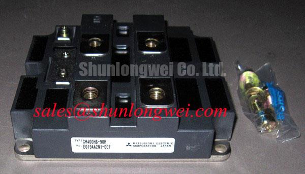
- Check the module marking against CM400HB-90H, then identify collector, emitter, and gate connections from the equipment schematic and terminal drawing.
- Inspect the heatsink contact surface, mounting hardware, and previous thermal interface imprint before preparing the replacement assembly.
- Check the disconnected gate-drive wiring for damaged insulation, loose contacts, and unintended continuity to the power circuit.
The Mitsubishi Electric CM400HB-90H is an IGBT module rated at 4500 V and 400 A, with the continuous-current rating specified at a case temperature of 80°C. For repair assessment, keep its electrical limits separate from the converter’s operating settings: the gate driver, cooling assembly, protection circuit, and busbar arrangement determine whether an installation remains within those limits.
The following values are Official Specifications. Package dimensions, terminal assignments, mounting torque, switching test conditions, and protection timing require the applicable manufacturer drawing and datasheet.
| Parameter | Symbol | Official Specification | Condition |
|---|---|---|---|
| Collector-emitter voltage | VCES | 4500 V | Maximum rating |
| Continuous collector current | IC | 400 A | Case temperature 80°C |
| Pulsed collector current | ICP | 800 A | Subject to applicable pulse limits |
| Typical collector-emitter saturation voltage | VCE(sat) | 3.8 V | Collector current 400 A; junction temperature 125°C |
| Gate-emitter voltage limit | VGES | ±20 V | Maximum rating, not a drive setting |
| Junction-to-case thermal resistance | Rth(j-c) | 0.045 °C/W | IGBT part |
| Maximum junction temperature | Tj max | 150°C | Maximum rating |
Remove the previous interface material and inspect both mating surfaces before applying a fresh thermal interface layer. As a Design Consideration, contamination, raised burrs, and incomplete contact can produce uneven heat transfer even when the external cooling circuit appears functional. Record the removed module’s contact imprint; it can help distinguish an assembly problem from a cooling-flow problem without treating either as a confirmed cause.
Control interface thickness using the selected material supplier’s application method and the module mounting instructions. A thicker layer is not automatically a better correction for uneven contact. Inspect heatsink flatness and assess baseplate curvature against the permitted mechanical tolerances rather than compensating with extra paste. Spread the material consistently, avoiding trapped air and dry contact regions, and use a repeatable application process for subsequent service work.
Seat the mounting screws progressively in the prescribed sequence, bringing the baseplate into contact without local forcing. Field Alert: Use the specified mounting torque and tightening sequence rather than tightening harder to compensate for an uneven thermal interface. Do not treat the module as a press-pack assembly or introduce disc-spring pressure calibration or double-sided cooling unless the approved mechanical design explicitly requires it.
The specified junction-to-case thermal resistance describes the IGBT portion, not the complete path to coolant or ambient air. As an Engineering Recommendation, evaluate case temperature together with current, duty cycle, and cooling conditions during commissioning. Keep the thermal assembly unchanged while comparing switching waveforms so that a contact improvement is not confused with a change in electrical switching loss.
Field Diagnostics & Commissioning: Unpowered Bench Screening: Multimeter Diode Checks in CM400HB-90H Topologies
Measure the isolated main-terminal paths in both polarities with the gate held in its defined off state using an approved handling arrangement. As a Design Consideration, a digital multimeter can reveal gross shorts or unexpected conduction, but its diode-test voltage cannot establish high-voltage blocking capability. Record polarity, instrument mode, and whether the module remains connected to any surrounding circuitry.
Identify the freewheeling path from the circuit diagram before interpreting a diode-mode reading. Where an antiparallel diode path is shown, compare its forward and reverse responses with the specified circuit behavior or a known-good assembly under equivalent conditions. Avoid assigning a universal forward-voltage threshold: instrument test current, temperature, and parallel components affect the result. An unexpected reading warrants isolation and repeat measurement, not an immediate single-cause diagnosis.
Check gate-to-emitter and gate-to-collector behavior with suitable low-energy instrumentation. A multimeter resistance check is a gross leakage screen, not a gate threshold measurement or proof of insulation integrity. Keep handling controlled, discharge the gate appropriately, and investigate unstable readings alongside cable contamination and driver-board loading. The ±20 V gate-emitter rating is an absolute boundary; it does not prescribe the operating gate-drive voltage.
Replacement assessment should compare blocking voltage, circuit configuration, mechanical fit, terminal layout, driver requirements, and switching behavior. The separately listed CM800HA-28H is a comparison reference, not an established direct replacement for CM400HB-90H; a shared manufacturer or similar designation does not establish interchangeability.
As an Engineering Recommendation, reserve reverse-recovery assessment for controlled powered testing. A static diode check cannot reveal recovery snappiness or the resulting switching-node ringing. Those observations belong to the commutation measurements discussed below, where probe placement and current direction can be documented.
Preventing Spurious Faults: Short-Circuit Energy Let-Through Matching Guidelines for CM400HB-90H
Trace the fault-current path from the DC-link capacitors through the module and protective devices before selecting or reassessing a semiconductor fuse. As a Design Consideration, fuse total-clearing I²t describes the fuse’s energy let-through under stated conditions; it is not interchangeable with an IGBT short-circuit withstand specification. The 800 A pulsed-current rating must not be used as a short-circuit survival rating.
Coordinate the driver’s fault detection and controlled turn-off with the upstream interruption system. Review detection blanking, propagation delay, turn-off behavior, and the energy available from the DC link using the converter’s approved protection design. A fast fuse can limit sustained fault energy, but fuse selection alone cannot guarantee that semiconductor damage or enclosure rupture will be prevented.
For nuisance trips, capture the fault indication alongside gate-emitter voltage, collector-emitter voltage, and current using appropriately rated measurement equipment. Check whether the event coincides with switching edges, current reversal, or driver-supply disturbance. As an Engineering Recommendation, investigate signal integrity and sensing references before extending blanking intervals; suppressing an indication without understanding its timing can obscure a genuine fault.
When evaluating compatibility with a high-speed rail or heavy freight locomotive traction inverter, engineers should compare the complete approved power-stage configuration. Where a regenerative braking chopper is involved, the braking resistor, switching duty, and DC-link protection determine the energy-handling requirement; the module’s current rating alone does not establish it. Maintain the equipment’s specified clearances and insulation arrangements when refitting busbars, protective covers, and sensing leads.
Use Mitsubishi Electric’s High-Voltage HVIGBT Modules resource for manufacturer product-family context, while retaining the exact device documentation and converter service instructions as the basis for protection coordination.
CM400HB-90H Thermal-Electrical Optimization: Mitigating Commutation Turn-Off Voltage Spikes Through Practical Tuning
Capture collector-emitter voltage and commutation current together to distinguish turn-off overshoot from diode-recovery-related ringing. As a Design Consideration, loop inductance produces additional voltage during rapid current change, while abrupt reverse-recovery current decay can excite the surrounding circuit. Establish probe bandwidth, voltage rating, and connection geometry before comparing traces; measurement-loop pickup can otherwise resemble a device transient.
Evaluate peak reverse-recovery current and the subsequent current-decay shape at the relevant current and temperature conditions. These are dynamic observations, not values that can be inferred from the static ratings table. Minimize unnecessary commutation-loop area within the approved mechanical layout, and check busbar joints and snubber connections for changes introduced during service.
If adjusting turn-on gate resistance is permitted, assess its effect on diode recovery, switching loss, and driver behavior together. As an Engineering Recommendation, change one controlled variable at a time and retain the original configuration as a documented reference. Slower switching can reduce some transient stress while increasing switching energy; the final setting belongs to the converter’s validated operating envelope.
An RC snubber should be evaluated against the measured ringing behavior, repetitive dissipation, and component voltage stress rather than selected from the module’s current rating. Complementary-switch dead time also requires waveform verification: insufficient separation risks overlapping conduction, while excessive separation can increase diode conduction. Neither adjustment should substitute for checking the actual gate signal at the module terminals.
The article The 1200 V CoolSiC™ MOSFET Advantage in Three-Phase Power Conversion provides related technology context, not CM400HB-90H-specific switching guidance. After any approved tuning change, repeat the relevant operating transitions and record voltage peaks, gate excursions, current behavior, and case temperature before returning the converter to service.