Content last revised on September 12, 2026
Assembly Integrity & Layout Architecture: Gate Drive Loop Geometry for CM450DX-24A
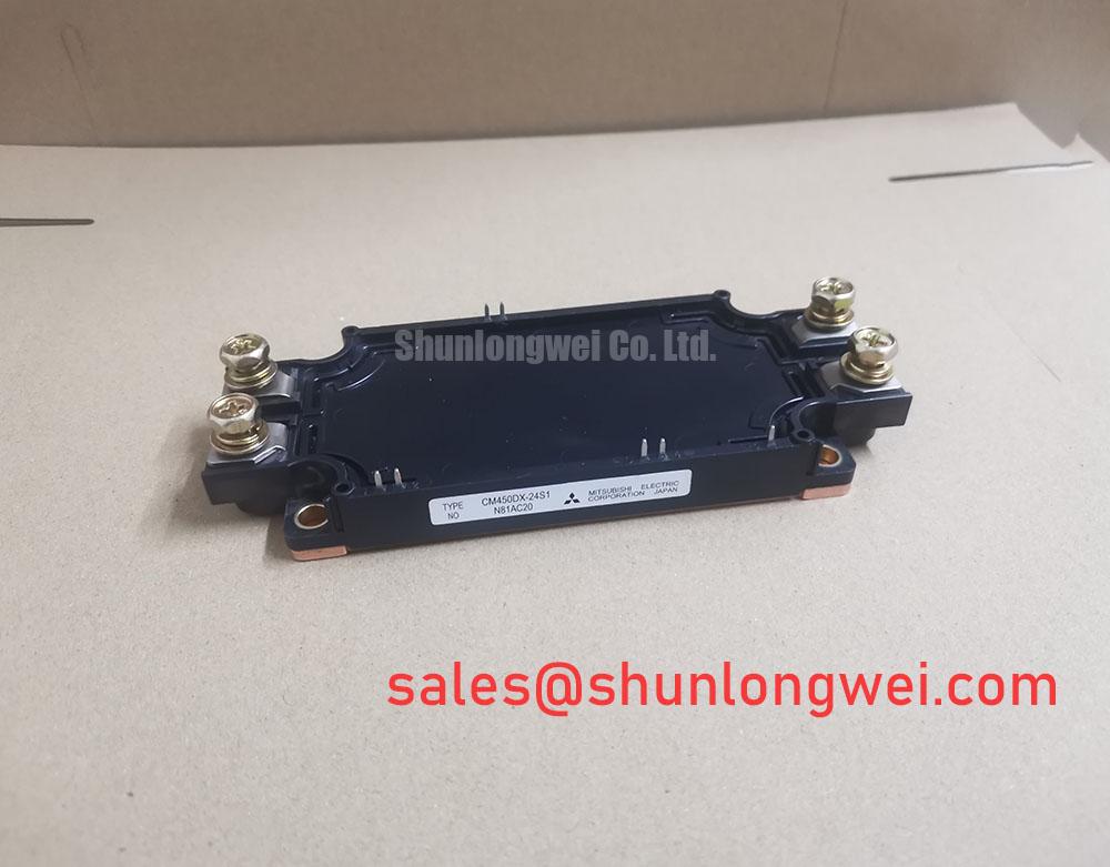
Inspect the removed assembly before fitting the CM450DX-24A. Look for heat-spreader contamination, uneven contact marks, damaged terminal hardware, carbon tracking around insulated areas, loosened busbar joints, and signs that the gate-control harness has been pulled or pinched. These observations do not identify a single failure mechanism, but they can reveal conditions worth correcting before a replacement power module is energized.
Gate-drive layout deserves separate attention from the main power-current path. A Design Consideration is to keep the gate-drive return path electrically compact and physically separated from high-current commutation paths wherever the original module terminal arrangement and driver design support that approach. Shared inductance between a fast-changing power current and a gate-control return can alter the voltage actually seen by the gate driver. During switching, that interaction can contribute to ringing, uneven turn-on behavior, or unwanted gate movement.
Where the original circuit provides separate control-return and power-emitter connections, the equipment layout should preserve their intended routing. The system engineer should verify connector pin assignments from the original inverter drawings rather than assuming that terminals with similar physical positions share the same electrical role. If an auxiliary control-return terminal is present in the original design, joining it casually into a long high-current return trace can defeat the purpose of the driver layout.
Busbar architecture also affects the practical switching environment around a 1200 V module. A laminated or closely coupled positive and negative DC-link path is commonly evaluated as a Design Consideration because reducing the loop area can reduce stray inductive effects during commutation. The objective is to limit turn-off overshoot and ringing while the system engineer verifies peak voltage margin against the installed DC-link voltage using appropriate switching measurements.
During fault investigation, compare the gate waveform and collector-emitter switching waveform with a known-good phase or a validated reference capture from the same equipment family. A waveform that differs from the expected shape may indicate a gate-loop routing issue, connection resistance, altered gate impedance, driver degradation, or a change in the power loop. It should not be assigned to one cause without measurement.
💡 Bench Tip: Keep the module and gate-driver assembly de-energized while connecting test leads, and compare cold-state readings only with the original circuit documentation or a known-good reference assembly.
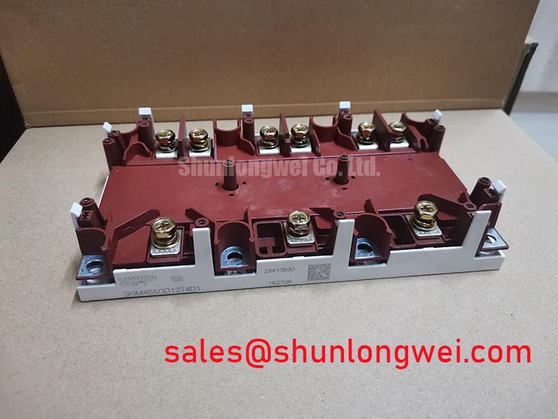
For repair planning, engineers sometimes evaluate the FF45017ME4 alongside the installed device as a separate reference part. Any possible substitution requires verified electrical, mechanical, terminal-layout, driver, protection, and thermal compatibility; matching current and voltage ratings alone is not sufficient.
CM450DX-24A Circuit Protection & Reliability: Dynamic Gate Impedance Control
The CM450DX-24A must be assessed as part of a complete switching system rather than as an isolated current-carrying element. The gate driver, DC-link layout, freewheeling path, snubber network, current sensing, and fault response all influence the electrical stress applied during normal commutation and abnormal operating events.
A Design Consideration for hard-switched converter stages is to review whether a dedicated gate pull-down path or active Miller-clamp function is present and working as intended. Fast collector voltage transitions can couple through internal device capacitances and disturb the off-state gate potential. The appropriate gate-drive arrangement, off-state bias method, and damping network depend on the original driver design, electrical isolation method, operating voltage, and measured switching behavior. Designers should validate these details on the actual converter rather than applying a universal gate-voltage prescription.
Practical interest in negative off-bias gate-drive circuits often arises when engineers are investigating unintended switching or poor immunity to high voltage transition rates. The article Evolution of Negative Off-Bias Gate Drive Circuits provides background for evaluating that driver strategy. It should be used as an engineering reference, not as proof that a particular negative bias value is suitable for this module or for the installed driver.
The commutating diode path also affects observed electrical noise. Reverse recovery behavior can influence current transition shape, voltage ringing, and radiated or conducted disturbance at system level. A snappy recovery event may require closer evaluation of the commutation loop, DC-link capacitor placement, snubber condition, and switching sequence. A Design Consideration is to inspect existing snubber capacitors, resistors, connections, and PCB traces for open circuits, thermal discoloration, or fractured solder joints before concluding that the power module is responsible for abnormal overshoot.
Fast semiconductor fuses and upstream protection devices should be reviewed against the converter manufacturer’s coordination data. Their prospective fault interruption behavior, I²t capability, conductor arrangement, and protective-device timing must be considered as a system. No module-level fault-energy limit, fuse rating, or protection time is asserted here because those values are not included in the stated official parameters for the CM450DX-24A.
In rectifier and complementary conversion stages, service teams may also encounter the 6MBI450U-120A-05. It should be treated as a separately specified component when reviewing the wider topology. The original converter schematic must establish whether it occupies a related stage and whether its control, cooling, and protection functions interact with the circuit containing the CM450DX-24A.
Field Diagnostics & Commissioning: Altitude and Voltage-Stress Assessment in CM450DX-24A Topologies
Before commissioning a repaired converter, record the actual DC-link voltage, incoming supply condition, cooling status, fault log, phase-current symmetry, and gate-driver supply behavior. These measurements establish a more useful baseline than attempting to infer equipment condition from a static semiconductor check alone. The 1200 V rating is an Official Datasheet Specification, but the acceptable operating margin must be determined by the converter manufacturer’s complete design requirements and the measured switching environment.
At elevated installation sites, system engineers may choose to review environmental, insulation, thermal, and semiconductor-stress conditions as part of a wider reliability assessment. Cosmic-ray and terrestrial-neutron effects, altitude-related voltage coordination, and single-event burnout behavior are high-risk reliability subjects that require manufacturer-specific qualification evidence or validated application data. No FIT rate, burnout probability, altitude threshold, or voltage-derating percentage is claimed for the CM450DX-24A here.
For equipment deployed in a multi-megawatt offshore or onshore wind turbine full-scale converter, a practical Engineering Recommendation is to verify the installed DC bus, switching peaks, enclosure environment, cooling circuit condition, insulation coordination, and control response against the turbine converter service documentation. This is an application example for compatibility evaluation, not a statement that the CM450DX-24A is certified or designated for every wind-converter platform.
Long motor or generator cable runs can introduce reflected-wave effects that change the voltage seen at remote machine terminals. Engineers investigating insulation alarms, repeated output filter failures, or irregular current-waveform behavior should inspect cable length, cable type, output reactor or filter condition, grounding arrangement, and measured terminal waveform. The cable reflection pattern is system-dependent, so a generic multiplier or fixed peak-voltage prediction should not be used as an acceptance criterion for this module.
When multiple power devices operate in parallel at system level, current sharing depends on matched electrical paths, gate-drive timing, thermal conditions, control-loop behavior, and the characteristics of the complete phase-leg assembly. Positive temperature-coefficient behavior is sometimes considered in parallel-device discussions, but it does not remove the need to measure dynamic sharing under controlled conditions. A current imbalance may indicate connection resistance, unequal cooling, gate timing variation, or another assembly-level condition that requires testing.
Static incoming checks should remain conservative. With the unit removed and safely discharged, use a meter’s diode mode only to compare expected semiconductor polarity paths with the original schematic or a known-good unit. A resistance or diode-mode result that differs from the reference may justify further investigation, but it does not independently establish dynamic blocking capability, switching performance, insulation integrity, or field reliability.
CM450DX-24A Operational Boundaries: Evaluating Desaturation Detection Limits
Desaturation protection is a gate-driver function that should be reviewed whenever a high-power converter has experienced an overcurrent trip, a blown semiconductor fuse, repeated gate-driver faults, or a damaged power stage. The driver typically monitors an indication related to the conducting switch voltage while the device is commanded on. The trip threshold, blanking interval, sensing path, isolation arrangement, and response sequence are determined by the complete driver design and must be verified from the original circuit information.
The CM450DX-24A current rating of 450 A should not be interpreted as a guaranteed short-circuit operating duration. Short-circuit safe-operating capability, if applicable, depends on conditions stated in the manufacturer’s complete documentation, including voltage, temperature, drive condition, fault type, and protection response. The provided official parameters do not establish a short-circuit withstand time, so no microsecond-level protection claim should be assigned to this part.
Where a driver uses soft turn-off after a desaturation event, its purpose is generally to manage the energy released from inductive current paths during interruption. An excessively abrupt fault turn-off can increase overvoltage stress, while an overly slow response can increase semiconductor energy dissipation. The correct response profile is therefore a system-specific design decision that requires validation with the installed DC-link, busbar, snubber, load inductance, and protection architecture.
Commissioning should begin with the converter manufacturer’s controlled startup sequence. Confirm the driver supply rails, control enable logic, interlock signals, current-feedback channels, temperature sensing, cooling flow or fan operation, and fault-reset sequence before applying full operating conditions. Oscilloscope probing should use an appropriate high-voltage differential method and a measurement setup that does not create an unintended ground path or excessive probe loop.
If desaturation protection trips during controlled testing, preserve the captured fault data before repeated restart attempts. Compare gate command, measured gate voltage, current-feedback response, DC-link voltage, and collector-emitter waveform where safely measurable. A trip can arise from a genuine load fault, gate-drive interruption, sensing error, excessive switching stress, poor connection, cooling issue, or control timing problem. The evidence should be reviewed as a set before the CM450DX-24A or any associated device is replaced.
Mitsubishi Electric’s global semiconductor device technology information provides manufacturer context for power-semiconductor product families. For this module, replacement acceptance should remain grounded in the confirmed 1200 V, 450 A, and package requirements together with the original equipment’s validated mechanical, electrical, and protection design.