Content last revised on September 10, 2026
Common-Mode Transient Immunity (CMTI > 100kV/us) in Harsh Industrial Environments
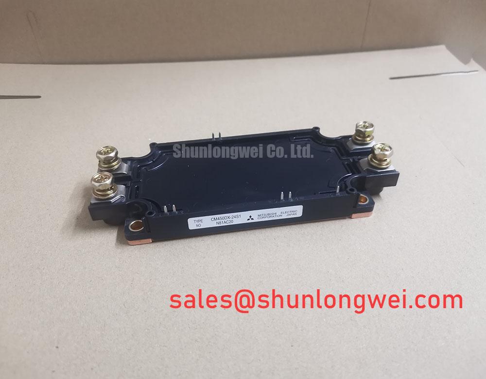
In high-capacity central solar photovoltaic (PV) inverters operating on utility grids, fast-switching transients are an unavoidable operating reality. When deploying the CM450DX-24S dual IGBT module from Mitsubishi Electric in transformerless 1500V DC-bus topologies (such as neutral-point clamped or multi-level conversion stages), the inverter bridge experiences rapid dv/dt transition rates often exceeding 15 kV/µs to 20 kV/µs across the collector-emitter terminals. These severe voltage steps inject displacement currents into galvanic isolation barriers, challenging the integrity of the gate drive circuitry.
To prevent catastrophic shoot-through events caused by false gate triggers, the gate drive interface must maintain a common-mode transient immunity (CMTI) rated well above 100 kV/µs (Design Consideration for severe industrial switching environments). When displacement currents penetrate isolation transformers or optocouplers with insufficient CMTI ratings, the resulting voltage ground bounce corrupts the control logic. This momentary disruption can force a high-side or low-side IGBT into parasitic conduction while the complementary switch is fully on, creating an immediate dead-time collapse.
Industrial gate driver designs paired with the CM450DX-24S utilize reinforced galvanic isolation barriers with continuous working insulation ratings exceeding 5.0 kVRMS to meet high-voltage clearance requirements under IEC 60664-1. On the PCB layout, physical clearance and creepage must strictly maintain a minimum of 12.5 mm across the isolation gap to withstand environmental pollution and salt-mist ingress often encountered in desert or coastal PV installations. Ground bounce mitigation also requires dedicated, low-capacitance isolated DC-DC power supplies (coupling capacitance under 1.5 pF) feeding each independent driver stage.
⚠️ Field Alert: During preventive maintenance of utility-scale inverters, inspect high-voltage isolation barriers for localized surface tracking, dust deposition, or dielectric discoloration. Conductive dust ingress combined with ambient humidity degrades creepage performance, causing localized micro-arcing and false desaturation trips during inverter ramping.
| Parameter | Symbol | Official Specification / Boundary | Engineering Maintenance Significance |
|---|---|---|---|
| Collector-Emitter Voltage | VCES | 1200 V (Official Datasheet Specification) | Provides essential voltage headroom for switching transient peaks and cosmic ray derating on utility DC rails. |
| Collector Current (DC) | IC | 450 A at TC = 119°C (Official Datasheet Specification) | Maintains massive current delivery under sustained elevated heatsink temperatures inside enclosed outdoor inverter cabinets. |
| Saturation Voltage | VCE(sat) | 1.80 V typ at 450 A, Tj = 25°C (Official Datasheet Specification) | Low conduction losses reduce thermal loading across continuous daily maximum-power-point tracking cycles. |
| Total Power Dissipation | Ptot | 3405 W at TC = 25°C (Official Datasheet Specification) | Represents maximum theoretical dissipation capability, dictating liquid/air cooling channel sizing. |
| Max Junction Temperature | Tjmax | 175°C (Official Datasheet Specification) | Ensures broad thermal margin during temporary grid faults and ambient temperature surges. |
Atmospheric Neutron Radiation Impact on 1200V/1700V Silicon Reliability
High-altitude utility-scale solar generation stations, frequently installed at elevations exceeding 2000 to 3000 meters in plateaus and mountainous zones, expose solid-state power devices to elevated fluxes of terrestrial atmospheric neutrons. High-energy neutrons colliding with the silicon crystal lattice can initiate localized impact ionization cascades within the high-field drift region of a reverse-biased IGBT. When the internal electric field is elevated, this interaction triggers a catastrophic, non-recoverable Single Event Burnout (SEB) within picoseconds.
The failure rate, quantified in Failures In Time (FIT, representing 1 failure per 109 component-hours), increases exponentially with the sustained DC-bus voltage applied across the collector-emitter terminals. While rated at a maximum Collector-Emitter Voltage of VCES = 1200V (Official Datasheet Specification), the CM450DX-24S must operate with deliberate DC-link voltage derating when deployed at high altitudes. In standard multi-level utility inverter architectures, maintaining the continuous static DC bias below 750V to 800V per 1200V switch stage provides an indispensable safety margin against cosmic ray-induced SEB failures (Design Consideration for high-altitude reliability).
To systematically troubleshoot power stage degradation and calculate lifespan margins under harsh environmental exposures, engineering teams frequently consult comprehensive failure analysis workflows outlined in the Field Engineer’s Handbook. Routine preventive maintenance at such sites must incorporate active dead-time buffer monitoring. When aging gate-driver optocouplers exhibit propagation delay drift, the software dead-time margin (tdead) can erode. Setting a baseline dead-time buffer between 2.5 µs and 3.5 µs (Typical Starting Point for 450A module architectures) prevents cross-conduction under fluctuating ambient temperature swings from -25°C to +55°C.
💡 Pro Tip: Implement complementary hardware gate interlocks directly on the secondary side of the driver board rather than relying solely on upstream DSP PWM signals. A hardware-level logic lockout physically prevents complementary gate signals from asserting concurrently if EMI or radiation upsets upstream logic.
Multi-Module Parallel Current Sharing & Positive Tempco Dynamic Balancing
Utility-scale central inverters demanding megawatt-level outputs regularly require multiple IGBT modules operating in parallel per phase leg. Static current distribution among paralleled modules is primarily governed by the Collector-Emitter Saturation Voltage, rated at VCE(sat) = 1.80V typical at 450A (Official Datasheet Specification). The 6th generation CSTBT silicon structure inside the CM450DX-24S features a positive temperature coefficient at nominal and elevated operating currents. As a particular die handles more current, its junction temperature rises, increasing its internal resistance and naturally shedding excess current to cooler adjacent modules.
For systems with reduced power density requirements or lower sub-assembly current branches, maintenance teams also encounter alternate module ratings such as the CM200DY-24E, which shares similar dual-pack form factors for modular sub-inverter stages. Dynamic current balancing during fast turn-on and turn-off transients, however, cannot rely on thermal coefficients alone. Dynamic imbalance is dominated by loop inductance discrepancies and gate circuit mismatches.
To achieve uniform dynamic current sharing across parallel branches, plant engineers and panel assemblers must implement strict symmetrical busbar geometry and matched gate loop traces:
- Individual Gate Resistors: Always drive each module through an independent, tightly toleranced gate turn-on (RG(on)) and gate turn-off (RG(off)) resistor. Never connect gate pins directly in parallel from a single gate resistor.
- Symmetrical DC-Link Laminated Busbars: Arrange DC-link busbars symmetrically so that stray inductances from each module to the main DC filter capacitors remain identical within a 5% tolerance window.
- Thermal Interface Material (TIM) Application: Maintain consistent thermal grease layer thickness between 60 µm and 80 µm across the copper baseplate to prevent local thermal hotspots (Design Consideration for baseplate mounting).
- Mounting Torque Calibration: Follow standardized mechanical fastening procedures, applying an M5 baseplate mounting torque of 2.5 to 3.5 N·m using a calibrated torque wrench in a diagonal two-step cross-pattern.
⚠️ Maintenance Note: Thermal paste dries out and degrades over multi-year duty cycles under continuous thermal cycling. Measure the thermal resistance rise via case temperature (TC) sensors annually. If the temperature differential between the baseplate and heatsink increases by more than 15% under identical load conditions, clean the surface thoroughly with isopropyl alcohol and reapply fresh non-curing thermal grease.
Kelvin Emitter Connection & Parasitic Inductance Minimization in High-Speed Switching
Fast switching transitions across 450A collector currents induce high di/dt rates through parasitic emitter lead inductances. In conventional power modules lacking an auxiliary emitter connection, the high main collector current share the same physical return path as the gate control circuit. The resulting induced voltage drop across the internal stray inductance actively opposes the gate drive voltage, throttling switching speed, increasing turn-on/turn-off switching energy losses (Eon / Eoff), and exciting high-frequency parasitic oscillations.
The CM450DX-24S eliminates this mutual coupling through a dedicated auxiliary Kelvin emitter terminal. By connecting the gate drive reference directly to the Kelvin emitter pin, the main load current is physically decoupled from the gate charge/discharge loop. This separation guarantees that the full gate drive voltage is delivered directly across the internal gate-emitter junction, maintaining sharp switching edges and stable desaturation (DESAT) sensing under severe load steps.
In centralized power conversion topologies where the inverter bridge interacts with input rectifier stages or peripheral auxiliary supplies, hardware configurations often pair these modules with half-bridge blocks like the CM400HA-12E to balance intermediate conversion links. As silicon technology continues to push temperature boundaries, next-generation power electronics are increasingly benchmarked against packaging innovations like Silver Sintering (Ag) Die-Attach for High Temperature SiC Modules and high-efficiency architectures represented by Mitsubishi Electric SiC Power Modules & SBDs.
When executing field repairs or testing gate drive boards connected to the CM450DX-24S, verify that gate drive twisted-pair cabling or direct PCB header connections maintain minimal loop area. A compact gate-emitter loop minimizes external magnetic flux pickup from adjacent high-current busbars, safeguarding the module's Maximum Junction Temperature rating of Tjmax = 175°C (Official Datasheet Specification) and preventing spurious gate ringing during emergency load disconnects.