



Content last revised on September 26, 2026
CM400HA1-34KA Operational Boundaries: Baseplate Contact and Mounting Screw Limits
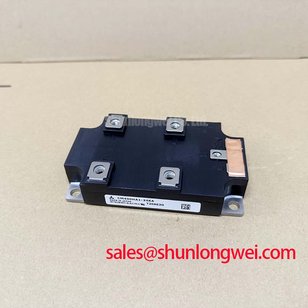
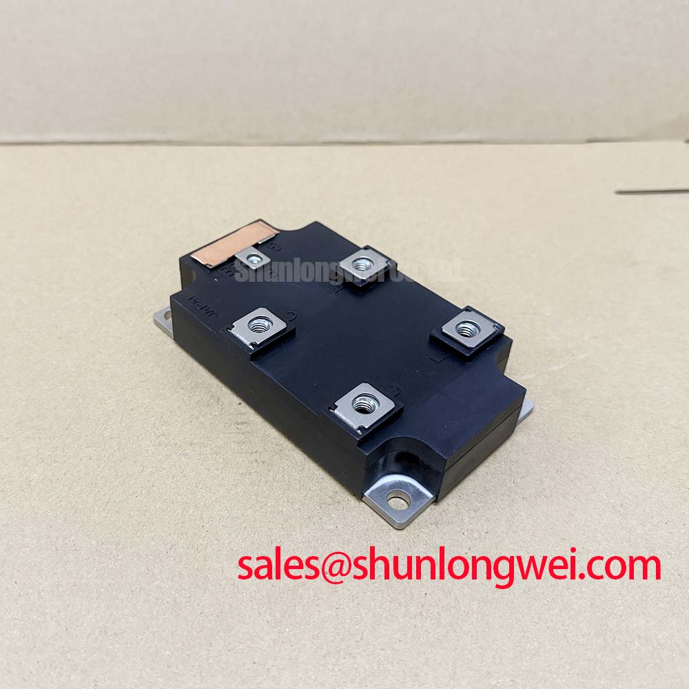
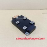
With the DC link isolated and verified discharged, compare the cold-state collector-to-emitter and gate-to-emitter readings of the installed CM400HA1-34KA with the equipment service record before removing its busbars. A multimeter can flag an obvious short or open connection, but it cannot establish switching performance or prove that a removed module will operate correctly under load. Record the terminal positions and fastener arrangement before disassembly; both matter when evaluating whether a replacement fits the existing assembly.
The CM400HA1-34KA is a Mitsubishi Electric IGBT module. Its collector-to-emitter voltage rating is 1700 V with the gate-to-emitter voltage at zero, and its continuous collector current rating is 400 A at a case temperature of 25 °C. The specified peak collector current is 800 A at the same case temperature for a 1 ms pulse. These are Official Datasheet Specifications, not permissions to operate indefinitely at peak current or at an uncontrolled case temperature.
| Parameter | Official Datasheet Specification | Stated condition |
|---|---|---|
| Collector-to-emitter voltage, VCES | 1700 V | VGE at 0 V |
| Gate-to-emitter voltage, VGES | ±20 V | VCE at 0 V |
| Collector current, IC | 400 A | Case temperature at 25 °C |
| Peak collector current, ICP | 800 A | Case temperature at 25 °C; 1 ms pulse |
| Collector power dissipation, PC | 2770 W | Case temperature at 25 °C |
| Operating junction temperature, Tj | −40 to +150 °C | Specified operating range |
Before seating the module, inspect the cooler contact area for residue, raised edges and fastener damage. As a Design Consideration, thermal interface material should fill surface irregularities without forming a thick, uneven layer. Check contact across the mounting surface and tighten the screws in a progressive sequence that avoids pulling one corner down first. Neither an allowable baseplate curvature nor a mounting torque is established by the specifications presented here; obtain those limits from the applicable Mitsubishi Electric mechanical drawing and the equipment assembly procedure rather than treating a general workshop value as a rating for this module.
Field alert: Do not choose mounting torque by feel; confirm the specified fastener and cooler instructions before tightening the module.
For an in-place change, compare the original unit’s outline, terminal locations, gate connections and cooler contact pattern against the replacement documentation before energizing the equipment. A matching current figure alone does not establish interchangeability. For example, 2MBI400TB-060-01 can be reviewed during an alternative-part assessment, but it should not be treated as a direct replacement without verifying voltage rating, circuit configuration, mechanical fit and drive compatibility.
Benchtop Waveform Tuning: Junction-to-Case Thermal Response on CM400HA1-34KA
After mechanical installation, establish a controlled test plan before returning the converter to its normal duty cycle. The module’s 2770 W power-dissipation figure is specified at a 25 °C case temperature; it is not a statement that the assembled cooler can remove that power continuously. Likewise, the −40 to +150 °C junction-temperature range sets an operating boundary, not a measured junction temperature during a particular pulse. Keep case-temperature measurement points, load conditions and switching records together so an apparent thermal problem can be distinguished from a changed operating condition.
A transient thermal estimate needs the module’s applicable junction-to-case thermal-impedance data and a realistic loss waveform. As an Engineering Calculation, a multi-RC model applies the time-varying device loss to the model’s thermal response, then adds the resulting junction rise to the measured or justified initial temperature. The specifications provided here do not include the thermal-impedance curve or RC coefficients, so a defensible peak-junction result cannot be calculated from the current and power ratings alone. For pulsed overload review, obtain that data and compare the modeled peak with the specified junction limit under the equipment’s actual cooling conditions.
On the switching bench, capture gate-to-emitter voltage and collector-to-emitter voltage at the module connections while observing the test setup’s measurement limits. As a Design Consideration, keep the high-current commutation loop compact to reduce inductive turn-off overshoot, then verify measured collector peaks against the DC-link level and the module’s 1700 V rating. A nearby snubber film capacitor can be considered when the converter topology calls for one, but its placement and value belong to system-level waveform validation rather than to a universal prescription for this part.
When evaluating the module in a utility-scale centralized battery energy storage power conversion system, trace the actual power path rather than assuming that every nearby power module performs the same function. A CM100DY-12E elsewhere in an equipment bill of materials is a separate module requiring its own topology and rating check; its presence does not establish an electrical relationship or interchangeability with the CM400HA1-34KA. Mitsubishi Electric’s power-device application information provides broader context for switching-device behavior, but the drive and thermal decisions for this installation must be checked against the specific module documentation and measured converter waveforms.
Transient Dynamics and Electrical Design: Fault Detection on CM400HA1-34KA
Before enabling a repaired power stage, review the driver schematic and confirm that its fault input, gate supply and turn-off path correspond to the installed module connections. The CM400HA1-34KA gate-to-emitter voltage limit is ±20 V at zero collector-to-emitter voltage, an Official Datasheet Specification. Probe the actual gate waveform under controlled switching conditions: a nominal driver supply does not by itself reveal ringing at the module terminals.
The specified gate-to-emitter threshold voltage is 5.5 to 8.5 V, with a 7.0 V typical value, measured at 40 mA collector current and 10 V collector-to-emitter voltage. Threshold is a measurement condition, not a recommended drive voltage for carrying 400 A. At that collector current, with gate-to-emitter voltage at 15 V, the specified collector-to-emitter saturation voltage is 2.70 V typical and 3.30 V maximum. Those conditions should accompany any comparison with a bench measurement; a reading taken at a different current or temperature is not a like-for-like acceptance test.
Desaturation monitoring is a Design Consideration for detecting abnormal collector voltage after a switching command, but its blanking interval, fault threshold and turn-off behavior must be selected against the complete driver and converter design. Do not infer a permitted short-circuit duration or a required two-stage turn-off timing from the ratings listed on this page. During commissioning, use suitably rated instrumentation to check whether the protection circuit responds to the conditions defined in the equipment service procedure and whether fault turn-off produces an unacceptable collector-voltage peak. Driver dead time also warrants verification against measured switching behavior so opposing devices are not commanded into conduction together.
If a fault persists, compare the command, measured gate waveform, collector voltage and protection output in time order instead of assigning one cause to a trip indication. The IGBT knowledge base offers background on the switching and diagnostic concepts; the decisive evidence for this repair is the equipment schematic and its captured waveforms.
CM400HA1-34KA Circuit Protection and Reliability: Checking the Emitter Return Path
Trace the gate-driver return from the driver output back to the module connection before changing any wiring. A dedicated auxiliary-emitter or Kelvin connection must not be assumed from the model name or the electrical ratings listed here. Check the manufacturer’s terminal drawing first. If that drawing identifies a separate emitter-sense terminal, route the driver return according to the documented connection so high-current emitter-path voltage drop is not unintentionally included in the gate-drive reference. If it does not, do not add an improvised sense connection.
As a Design Consideration, minimize gate-loop area and unintended coupling to the power path when investigating gate oscillation. Compare waveforms at the driver and at accessible module terminals under the same controlled test condition; a difference may point toward connection impedance or layout effects, but it does not identify a single failed part. Inspect terminal tightness and return-path continuity before altering damping components. Any change to the driver network should be checked against the resulting gate-voltage peaks, turn-off collector overshoot and the equipment’s protection response.
For a cold-state leakage check, keep the datasheet test conditions distinct from an ordinary multimeter test. The official maximum gate-to-emitter leakage current is 0.5 µA at ±20 V gate-to-emitter voltage with collector-to-emitter voltage at zero. The official maximum collector-to-emitter cutoff current is 1.0 mA when collector-to-emitter voltage equals the specified 1700 V rating and gate-to-emitter voltage is zero. A handheld resistance reading does not reproduce either condition. Where those measurements are necessary, use an appropriate controlled test setup and compare the result with the stated limits and the equipment’s isolation procedure.