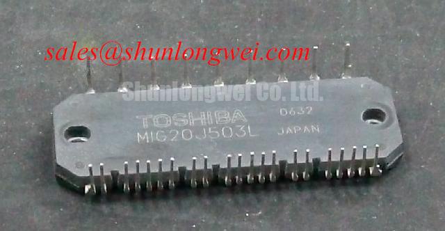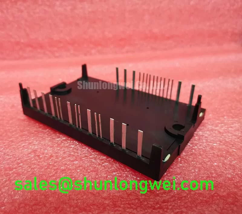
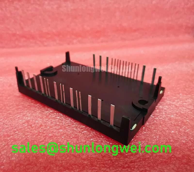


Content last revised on October 11, 2026
J2-Q04A-D Installation and Service Checks
Before applying power to an industrial inverter welder or medium frequency induction heater, isolate the DC link and inspect the J2-Q04A-D installation for loose power connections, damaged insulation, abnormal terminal contamination, and evidence of thermal overstress. This Fuji Electric device is identified as a Power Transistor / Darlington Module with a Standard Industrial Rating for working voltage, Standard Operating Current, and a Power Transistor Module package. These are the available product classification parameters and should be matched with the equipment service documentation before replacement.
For bench work, record the original conductor routing before removing the module. The base or control return path, main power emitter path, DC link connection, and heat spreader contact all influence switching behavior. A replacement that fits mechanically can still produce excessive ringing if the control loop, busbar geometry, or terminal return arrangement changes.
Preventing Spurious Faults: Long Motor Lead Reflected Wave Voltage Guidelines for J2-Q04A-D
Long motor leads behave as a transmission path rather than a simple wire, so impedance mismatch can reflect switching energy back toward the inverter bridge. In severe cases, the terminal voltage transient can approach twice the DC link voltage at the load end or module terminals, depending on cable length, propagation delay, termination, and switching edge rate. This is a system interaction, not a standalone rating of the J2-Q04A-D.
When an industrial inverter welder or induction heating power stage shows intermittent overvoltage trips, inspect the complete output path. Check whether the cable arrangement has changed from the original machine design, whether a motor lead has been extended, and whether an output reactor, dv/dt filter, or common mode component has been bypassed during service. A clamp meter may show normal current while a differential voltage probe reveals severe switching overshoot.
Design Consideration: output filtering should be selected from the cable impedance, switching frequency, motor insulation requirement, and measured peak voltage. The filter or choke must not be chosen only from the nominal current printed on the machine nameplate. Verify the filter response with the actual cable and load, then observe the module terminal waveform during acceleration, regeneration, and rapid load changes.
Keep the high current commutation loop compact and physically separated from sensitive control wiring. Parallel runs between output conductors and base or auxiliary return conductors can increase capacitive coupling and trigger nuisance protection. The system engineer should establish clearance and creepage according to the applicable equipment insulation design, contamination environment, working voltage, and enclosure arrangement.
For service comparison, the related 6DI10A-050 can be reviewed as a separate Fuji Electric module reference. It should not be treated as a direct substitute until voltage class, current capability, terminal arrangement, switching behavior, mounting geometry, and base-drive requirements have been checked against the original circuit.
Benchtop Waveform Tuning: Mitigating Stress from Control-Terminal Voltage Spikes on J2-Q04A-D
High dv/dt at the collector can couple through the device output capacitance and surrounding parasitic capacitance into the control circuit. The resulting transient may disturb the base-emitter voltage or control reference and contribute to unwanted conduction in a bridge leg. A short base-drive loop, controlled base resistance, and a driver with a low-impedance turn-off path are the first areas to examine.
Active Miller clamping and negative gate bias are not generic controls for a Darlington power transistor module. Any control-terminal clamp or reverse base-emitter bias must be considered only where the module and driver documentation support it, with the actual value determined by the device limits, driver capability, fault response, and original equipment design. Values discussed for other industrial switching devices must not be applied to this model without confirming the device and driver documentation.
High side drive integrity deserves separate attention. A bootstrap supply must provide the required base-drive current for the complete high side switching sequence while also supplying driver quiescent current, leakage, refresh losses, and transient demand. Select the capacitor and charging path from the required base-drive conditions, maximum on time, switching duty cycle, temperature, and acceptable supply ripple. Diode reverse recovery can inject a disturbance into the driver supply, so the diode and local decoupling arrangement should be evaluated with the intended switching frequency.
| Evaluation item | J2-Q04A-D | 6DI10A-050 |
|---|---|---|
| Manufacturer | Fuji Electric | Fuji Electric |
| Product category | Power Transistor / Darlington Module | Consult Datasheet |
| Working voltage | Standard Industrial Rating | Consult Datasheet |
| Operating current | Standard Operating Current | Consult Datasheet |
| Package | Power Transistor Module | Consult Datasheet |
| Replacement status | System compatibility review required | Independent compatibility review required |
The table is a screening aid, not a substitution approval. Use a differential probe at the module terminals and a suitable isolated probe at the control terminals. Compare turn-off base-emitter behavior, collector-voltage transition, storage behavior, collector-voltage overshoot, dead time, and driver supply stability under the same load condition. The Fuji Electric Power Semiconductors Portal and the Fuji Electric PIM Power Integrated Module reference provide useful manufacturer context for power module families, while the exact drive arrangement remains equipment specific.
J2-Q04A-D Circuit Protection & Reliability: Calibrating Type 2 Coordination for Power Transistor Module Protection
Semiconductor fuse coordination must be established from the fuse total clearing I2t, prospective DC link fault current, circuit inductance, fuse voltage rating, and the module short-circuit withstand characteristics. A fuse selected only from normal operating current may not interrupt a DC link fault quickly enough, while an improperly coordinated fuse can introduce excessive let-through energy before clearing.
For a Type 2 coordination review, map the protection chain from the DC link capacitor through the busbar, fuse, switching bridge, and return path. Include capacitor discharge energy and stray inductance in the fault assessment. The physical fuse position matters because the section of busbar between the fuse and module can continue delivering destructive energy after the fuse element has started to operate.
Check the fuse manufacturer clearing curves at the actual prospective fault current rather than relying on a nominal time label. The resulting energy must be compared with the module and complete power stage limits specified by the equipment design. Case integrity, terminal heating, busbar spacing, and enclosure pressure relief are system safety subjects and should be assessed under the applicable machinery and electrical safety requirements.
Regenerative braking adds another stress path. During deceleration, the DC link can rise as motor or load energy returns to the bus. The braking chopper, resistor, control threshold, and thermal duty must be evaluated together. A resistor that absorbs a short pulse may not survive repeated medium frequency operation, and a chopper fault can expose the J2-Q04A-D power stage to an abnormal DC link condition.
During fault investigation, inspect fuse contact pressure, discoloration around busbar joints, capacitor venting, and signs of repeated short-duration trips. Replace protective components according to the original coordination study and do not bridge a semiconductor fuse during testing. Where wide-bandgap devices are being considered elsewhere in the same power platform, the engineering principles in this Wide Bandgap Revolution guide can help explain the different switching stress and layout considerations without implying interchangeability with this module.
Transient Dynamics & Electrical Design: Auxiliary Kelvin Emitter Versus Main Power Emitter on J2-Q04A-D
Separate the control return from the high-current emitter path whenever the module provides an auxiliary emitter or dedicated low-current return. The main emitter carries commutation current and develops a transient voltage across its stray inductance. If that same conductor is used as the driver reference, the driver can see ground bounce and unintentionally alter the control voltage.
Trace the driver return directly to the appropriate control reference point and keep it away from the high-current busbar loop. Do not assume that two physically adjacent terminals have identical electrical roles. Confirm the terminal identity from the original Fuji Electric documentation and the equipment schematic before wiring a replacement. A wiring error can leave the module apparently functional at low power while producing unstable switching at load.
Use a short, tightly coupled base-drive and return path, with the base resistor located close to the module or driver interface selected by the original design. Any ferrite bead, damping network, control-terminal clamp, or reverse-bias circuit should be evaluated for its effect on turn-on delay, turn-off delay, collector-voltage transition, storage behavior, and protection timing. The final arrangement is determined by measured waveforms and the complete switching loop, not by package appearance alone.
Mechanical installation also affects electrical reliability because uneven baseplate contact raises thermal resistance and changes the operating temperature of the power stage. Clean the mounting surfaces, apply a uniform thin thermal interface layer, and tighten fasteners in the equipment manufacturer’s specified sequence and torque. 🔧 Field Alert: Disconnect the DC link and verify discharge before removing control or power wiring, then confirm the original terminal function before reconnecting the replacement module.
For procurement and repair records, retain the J2-Q04A-D manufacturer marking, package description, application position, measured fault symptoms, and the control board revision. This information lets the next engineer distinguish a module replacement issue from a changed base drive, altered cable path, or degraded protection circuit.