

Content last revised on October 16, 2026
Preventing Spurious Faults: Separating Driver Return from Main Current Guidelines for MIG20J503L
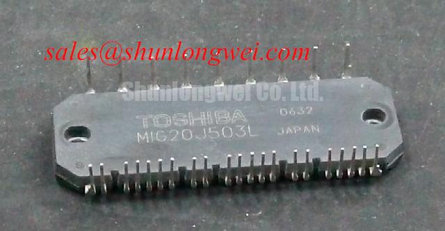
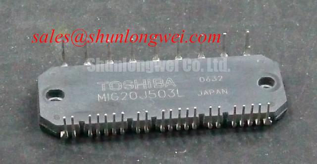
MIG20J503L is a Toshiba Intelligent Power Module. Exact voltage and current ratings, their applicable conditions, and package details should be taken from the applicable Toshiba documentation used for the equipment service record.
| Item | Specification status |
|---|---|
| Manufacturer | Toshiba |
| Model | MIG20J503L |
| Voltage rating | Refer to the applicable Toshiba datasheet |
| Rated current | Refer to the applicable Toshiba datasheet and rating conditions |
| Package details | Refer to the applicable Toshiba package drawing |
| Product category | IPM, Intelligent Power Module |
- Confirm cold state impedance between the main power terminals and compare the result with an approved reference unit.
- Inspect the mounting interface for baseplate contact, heatsink flatness, contamination, and uneven thermal interface material.
- Trace the driver or control reference return separately from the high current path before applying switching power.
- Verify driver isolation, bootstrap operation where used, and control board clearances before connecting the motor.
Separate the driver or control reference return from the main load current path before investigating unexplained turn on, gate ringing, or intermittent protection trips around MIG20J503L. In an inverter application, the emitter connection carrying motor current can develop a rapidly changing voltage relative to the control ground. If the driver return shares that path, the control circuit can interpret the resulting ground movement as a gate command or an undervoltage event.
Start at the physical terminals rather than relying only on the schematic. Identify the main power conductors, then locate the control reference or auxiliary emitter connection, if provided, defined for the driver interface. The reference return should travel directly to the appropriate driver or control reference with a compact loop. It should not be routed through the copper region used by the high current emitter connection, braking path, or motor return. The exact terminal identity must follow the package drawing associated with the installed part revision.
A useful field check is to temporarily observe the driver reference and, where accessible, the gate to auxiliary emitter voltage with differential probes while the inverter operates under a controlled low energy condition. Compare the waveform at accessible module terminals with the waveform measured at the corresponding driver output. A difference between these locations can indicate common impedance, excessive loop area, probe reference error, or an isolation interface problem. The result should be compared with a known good signal path rather than judged from a single voltage threshold.
Where the design provides external gate connections, keep the gate loop compact and place the gate resistance, clamp network, and driver return according to the switching direction being controlled. Gate loop parasitic inductance interacts with gate capacitance and Miller current, so a long return conductor can produce oscillation even when the static gate voltage appears correct. For an integrated driver interface, follow the manufacturer’s connection guidance. The control and power copper should cross only where necessary, preferably with a clear reference strategy that prevents high di/dt current from entering the logic return.
In a motor drive application, also inspect the isolation barrier and communication reference during motor acceleration and regenerative braking. An optocoupler or digital isolator may experience common mode transient stress when the switching node moves quickly. Its CMTI capability, supply decoupling, and placement must be evaluated against the actual inverter transition. The module itself should not be described as independently meeting a complete machine EMC requirement; system level cabling, enclosure, grounding, and filtering determine that result.
Any comparison with another module, such as PM75CSD120, requires independent verification of voltage and current ratings, pin arrangement, switching behavior, protection interface, thermal path, and controller settings before any substitution is approved. No replacement relationship is established here.
🔧 Bench Diagnostic: De energize the inverter and discharge all stored energy before disconnecting or reconnecting gate driver wiring.
Transient Dynamics & Electrical Design: Heatsink Surface Flatness and Thermal Grease on MIG20J503L
Inspect the module mounting surface and heatsink interface as a mechanical assembly, because uneven contact can create local thermal resistance that is invisible during a brief no load test. Clean both mating surfaces with a suitable process, remove particles and burrs, and check the heatsink for rocking or visible distortion before applying thermal interface material.
The interface compound should form a continuous, thin film after compression rather than a thick cushion. A practical engineering consideration is to use a controlled application method that targets an even distribution in the approximate range of 50 to 80 µm, provided that the compound supplier and module assembly instructions support that process. This range is a general assembly consideration, not a Toshiba factory specification for every installation.
Install the module without sliding it across the prepared surface. Bring the fasteners down progressively using the sequence specified in the module assembly instructions so the mounting surface seats evenly. The final tightening torque must follow the module mechanical documentation and the selected fastener system. Excessive force can distort the package or substrate, while insufficient force can leave voids in the thermal path. Check the finished assembly for uniform seating rather than assuming that equal screw rotation produced equal pressure.
Where a bootstrap supply is used, its capacitor has to support the high side driver’s charge demand, quiescent current, leakage, and intended maximum high side on time. Designers should calculate the required capacitance from the applicable driver operating conditions, including gate charge where supplied by that capacitor, then validate the supply voltage at the driver pins during repetitive switching. The capacitor location, diode or charging path, and return conductor are part of the same high frequency loop. Bootstrap operation must also provide sufficient opportunities for recharging.
In a motor drive inverter, long motor cables can behave as transmission structures at fast switching edges. Reflections may increase the voltage appearing at the motor terminals and affect the switching node, especially when cable impedance, motor winding characteristics, and termination conditions are not coordinated. Filtering should be selected from measured common mode and differential mode behavior, with attention to filter resonance and the resulting gate drive disturbance. The system engineer should verify peak voltage and current margins during controlled switching tests rather than relying on the nominal DC bus value alone.
The insulation spacing around the power terminals and switching nodes should be reviewed against the working voltage, pollution environment, material group, altitude, and applicable installation category. The principles of insulation coordination described in IEC 60664 provide a useful framework for that review. They do not replace the clearance and creepage requirements of the complete equipment standard.
For system topology work, the rectifier or front end is a separate design block. If another power module, such as PM150DSA120, is considered elsewhere in the converter, its circuit configuration, ratings, and switching behavior must match the intended function. Its presence does not establish electrical compatibility with MIG20J503L; bus voltage, commutation paths, protection timing, and thermal loading still require system verification.
Benchtop Waveform Tuning: Mitigating Stress via Transient Thermal Impedance on MIG20J503L
Use the applicable transient thermal impedance profile, where available, when a short overload or regenerative pulse produces heating that is not represented by steady state thermal resistance. The relevant junction temperature is influenced by pulse width, duty cycle, starting case temperature, mounting interface, and the thermal response of the heatsink. A multi RC representation is useful because the short time response and the longer case to heatsink response do not occur at the same rate.
For a benchtop evaluation, record the case temperature at the specified measurement location, the device voltage and current waveforms, and the pulse timing at the same operating condition. The resulting semiconductor power loss profile can then be applied to the applicable transient thermal impedance model using pulse superposition or an equivalent thermal calculation. The resulting junction temperature estimate should include switching losses and the initial thermal state from earlier pulses, not just the energy of the final pulse.
Waveform tuning should begin with controlled switching at low energy and adequate dead time, then expand the operating envelope only after the accessible gate or control waveforms, collector emitter voltage, and current overlap are stable. Gate resistance, driver impedance, layout inductance, Miller response, and the external commutation loop all influence the observed overshoot. Adjustments should be made one variable at a time so that reduced ringing is not confused with increased switching loss. Changes to gate resistance or driver impedance apply only where the module interface permits them.
Probe technique is part of the measurement. Use a suitable differential voltage probe with a short connection at the module terminals and position the current sensor so that the measured loop represents the actual commutation path. A long oscilloscope ground lead can introduce ringing that is not present in the power stage. Where external gate connections are available, repeat the measurement at the driver output and at the module gate terminals to separate control wiring effects from power loop behavior.
The thermal model should be checked against case temperature rise over repeated pulses and against the cooling system’s settled behavior. If the estimated junction temperature approaches the applicable operating limit, reduce electrical or thermal stress through system level changes such as switching profile adjustment, improved airflow, reduced commutation loop impedance, or a revised heatsink arrangement. These are engineering options, not fixed prescriptions for this model.
Engineers working on the gate drive, thermal path, and converter topology can use the related IGBT Design & Integration reference as a broader technical aid. Packaging research such as flip chip and copper pillar interconnect technology explains how low parasitic interconnect concepts are studied in semiconductor packaging, but it should not be treated as a confirmed internal construction detail of MIG20J503L.