Content last revised on September 19, 2026
Preventing Spurious Faults: Cosmic Ray Robustness: Voltage Derating Guidelines for CM75E3Y-12E
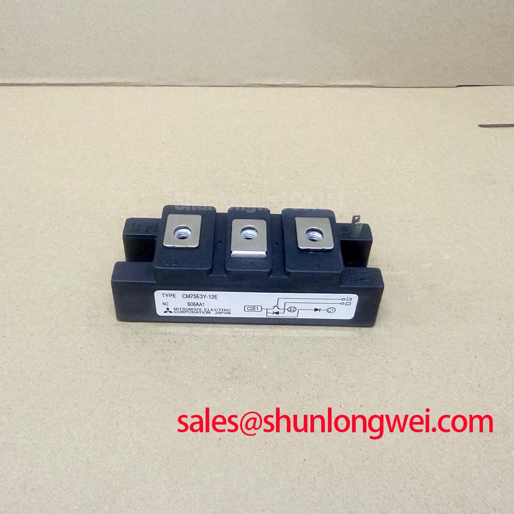
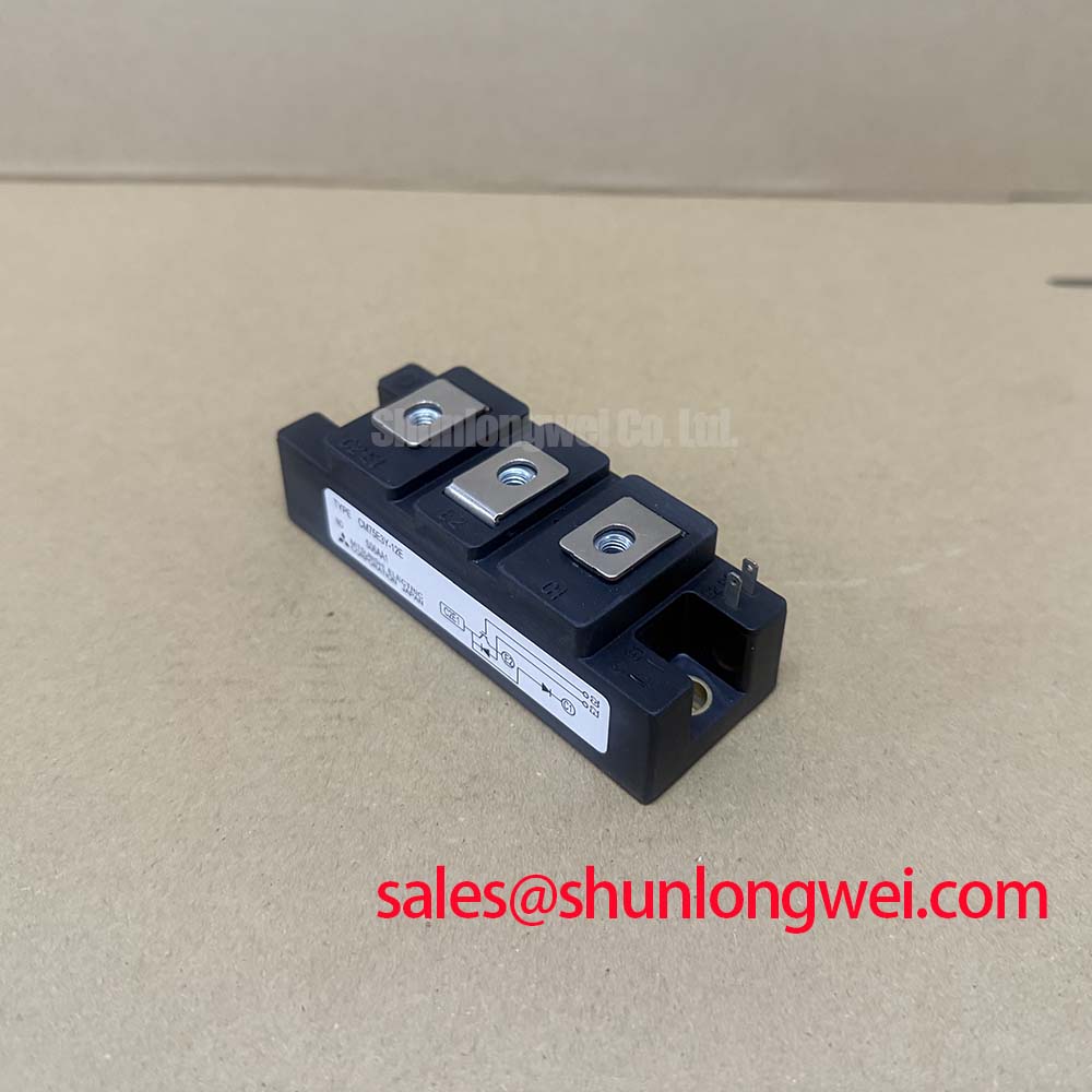
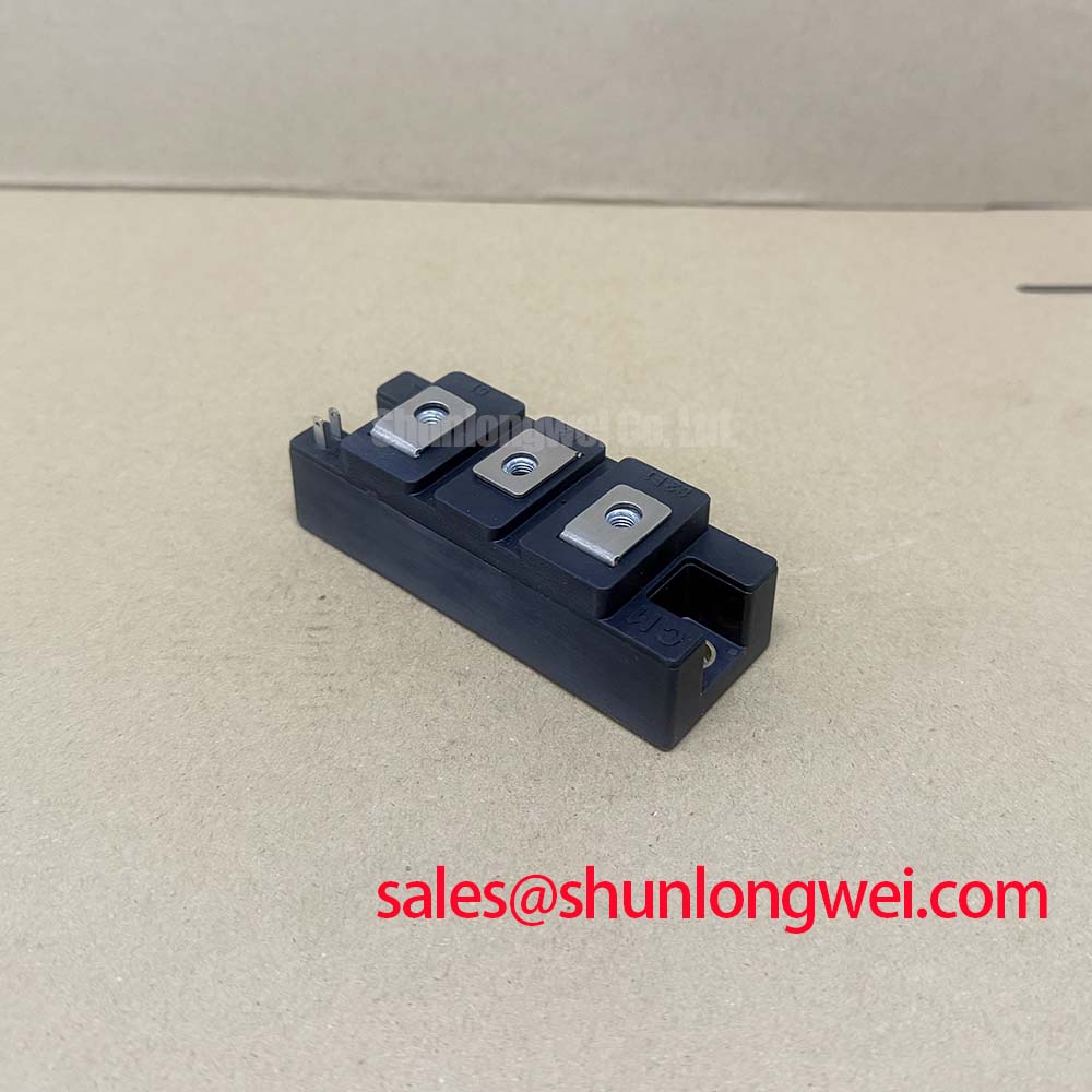
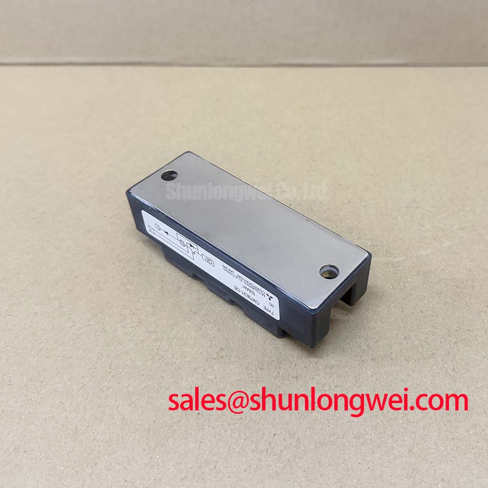
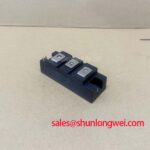
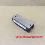
With the drive isolated, begin by checking the CM75E3Y-12E power terminals for unintended low resistance paths, then inspect the module body, terminal hardware, busbar contact faces, and heatsink interface for looseness, heat discoloration, or mechanical damage before applying power. This Mitsubishi Electric power semiconductor is a 600 V, 75 A IGBT Module, rated at VCES = 600 V and IC = 75 A as Official Datasheet Specifications. For a repair decision, those ratings must be matched against the original inverter schematic, DC bus operating range, gate driver arrangement, cooling assembly, and terminal geometry rather than compared by current rating alone.
| Parameter | Specification | Classification |
|---|---|---|
| Product model | CM75E3Y-12E | Official identification |
| Manufacturer | Mitsubishi Electric | Official identification |
| Collector emitter voltage rating | 600 V | Official Datasheet Specification |
| Current rating | 75 A | Official Datasheet Specification |
| Package | Module | Official Datasheet Specification |
For manufacturer technology context, consult Mitsubishi Electric Power Semiconductors and High Power Modules. The original equipment documentation remains the controlling reference for terminal assignment, gate drive polarity, protection thresholds, switching conditions, and mechanical fastening requirements for this exact installation.
Confirm the actual DC bus voltage at the module terminals before treating an intermittent inverter trip as a device issue. The 600 V voltage rating is an Official Datasheet Specification, but it is not a complete description of the voltage stress seen during a switching event. Cable inductance, laminated busbar construction, DC link capacitor position, braking activity, and probe location can all affect the peak collector emitter voltage measured in service.
At elevated installation sites, terrestrial neutron exposure is sometimes considered during system reliability assessment. No model specific cosmic ray, single event burnout, altitude derating, or FIT figure is stated here because such values require a manufacturer source and a defined operating condition. A Design Consideration is to treat altitude and environmental exposure as system level validation subjects. Engineers should review the inverter maker’s environmental limits, measure DC bus excursions under representative load transitions, and verify that observed switching peaks remain inside the system’s validated voltage envelope.
Do not infer a cosmic ray event from a failed module alone. A service investigation is more useful when it starts with retained fault records, bus voltage capture where available, braking resistor continuity, contactor behavior, line surge history, and the condition of the output cable. If several drives show similar events after a site change, examine installation altitude, incoming power disturbance, enclosure contamination, cooling airflow, and grounding topology before assigning a single cause.
Clearance and creepage distances belong to the complete drive assembly, not to a generic rule applied to the module. Design Consideration: maintain clean, dry insulating surfaces around exposed bus conductors and ensure that busbars, terminal covers, and control wiring retain the clearances required by the equipment’s applicable standard. Carbon tracking, conductive dust, and moisture can produce misleading gate driver faults that resemble power stage instability.
When evaluating a heavier rated alternative during an equipment redesign, the CM300DXDX1-24A can be reviewed as a separate module reference. Its suitability cannot be assumed from its model name or current class. Terminal arrangement, voltage class, internal circuit arrangement, driver compatibility, protection settings, thermal path, and fault response all require direct comparison with the original drive design.
CM75E3Y-12E Thermal-Electrical Optimization: Transmission Line Impedance Mismatch: Practical Tuning
On a heavy duty variable frequency AC motor drive, place the oscilloscope measurement focus at the module side of the DC link and at the motor output when troubleshooting unexplained overvoltage or motor insulation alarms. Long motor leads can behave as transmission lines. Their reflected wave behavior can raise motor terminal stress substantially above the inverter output waveform, and a peak near twice the DC bus voltage is possible under particular cable and load conditions. That is a system phenomenon, not an additional rating claim for the CM75E3Y-12E.
Engineering Recommendation: investigate cable length, cable construction, motor terminal waveform, switching pattern, and output filter condition together. A dv/dt filter, sine wave filter, or output choke may be evaluated where measured reflected voltage or bearing current concerns justify it. Filter selection must be determined by the drive controller, motor characteristics, cable route, load duty, and measured thermal results. Adding a filter without checking its impedance and thermal behavior can shift rather than remove the problem.
At the inverter side, minimize the commutation loop inductance between the DC link capacitors, bus conductors, and module terminals to suppress turn off overshoot. Keep the DC link capacitor connection mechanically secure and electrically short in the physical layout permitted by the original design. A film snubber capacitor, where the original design provides one, should be connected and inspected exactly as shown in the equipment documentation. Its role is to support high frequency current locally; it does not replace the energy storage function of the main DC link capacitors.
During field repair, inspect the braking chopper path and braking resistor assembly if the DC bus rises during deceleration. Regenerative energy must be handled by the drive’s intended braking or regeneration system. A disconnected resistor, defective braking transistor circuit, incorrect parameter set, or load with high inertia may each contribute to overvoltage trips. Record bus voltage, commanded speed change, and fault timing before replacing power hardware.
⚠️ Field Alert: Isolate and discharge the DC link, then follow the equipment manufacturer’s specified terminal torque and apply a thin, even thermal interface layer before fastening the module to the heatsink.
For wider power conversion context, The 1200 V CoolSiC™ MOSFET Advantage in Three discusses switching and system architecture considerations in three phase conversion. It is useful as background reading, but it does not alter the official 600 V and 75 A specifications of this Mitsubishi Electric module.
Preventing Spurious Faults: Active Miller Clamp Implementation Guidelines for CM75E3Y-12E
Before changing gate driver parts, compare each gate command waveform with the original drive’s known good channel under controlled conditions. A fast collector voltage transition can couple energy through internal capacitances and wiring parasitics into an inactive gate loop. If the gate is allowed to rise enough, an unintended turn on event may occur. This can appear as a sporadic overcurrent trip, asymmetric heating, damaged gate driver components, or a fault that only occurs at a particular output current and bus voltage.
An active Miller clamp is a gate driver function that provides a low impedance gate emitter path after turn off, helping the driver resist unwanted gate rise during high dv/dt transitions. Whether the existing CM75E3Y-12E installation uses such a function must be verified from the original gate driver circuit. It should not be added as an isolated modification without reviewing the driver supply arrangement, isolation scheme, desaturation or overcurrent protection, fault shutdown behavior, and gate loop layout.
Negative gate bias is also a Design Consideration used in some IGBT drive systems to increase turn off immunity. The required voltage is system determined and must follow the module and gate driver documentation. Applying an arbitrary negative bias can exceed gate limits, change switching stress, interfere with fault protection, or create gate driver supply problems. Verify gate emitter voltage at the module connection, not only at the driver board, because lead inductance can make the observed waveform materially different.
A practical diagnostic sequence starts with the machine de energized. Check continuity of the gate drive harness, inspect connector retention, and compare gate resistor locations and fitted values across parallel channels. Then, under a controlled powered test, use correctly rated differential measurement equipment to compare gate voltage, collector emitter voltage, and current feedback timing. If one channel behaves differently, inspect its driver supply stability and command return path. Do not treat a changed waveform as proof of a failed IGBT until the control and measurement paths have been checked.
Dead time is another system determined protection variable. Too little separation between complementary commands can allow cross conduction; excessive separation can affect waveform quality and torque behavior. Engineering Recommendation: retain the original validated dead time after a like for like replacement, then verify switching behavior according to the drive manufacturer’s commissioning procedure. Changes to dead time, gate resistance, or clamp behavior should be evaluated as a complete switching system, with voltage overshoot, current shape, thermal response, and protection timing observed together.
The Mitsubishi Electric Global Semiconductor Device Technologies resource provides manufacturer level semiconductor context. For a repair, use the specific original documentation to confirm every driver interface detail not stated in the provided official parameters.
CM75E3Y-12E Circuit Protection & Reliability: Evaluating Thermal Capacitance vs Heat Sink
Begin thermal troubleshooting by checking the physical heat path rather than estimating junction temperature from the heatsink surface alone. The module baseplate, thermal interface material, heatsink flatness, fan operation, airflow route, and ambient air temperature all influence the result. The CM75E3Y-12E is rated at 75 A, yet actual current capability in a drive depends on switching conditions, pulse duty, cooling performance, and the equipment’s protection calibration.
Thermal capacitance describes the temporary ability of the module structure to absorb energy during a pulse before heat reaches the case and heatsink. In heavy pulsed operation, junction temperature can rise much faster than a remote heatsink sensor indicates. Multi RC thermal impedance models are used by system designers to estimate that transient response, but a valid calculation requires model data, loss data, pulse duration, case condition, and initial temperature from the applicable manufacturer documentation. Without those inputs, a numeric junction margin would be speculative.
Engineering Recommendation: verify the heatsink contact surface for burrs, corrosion, distortion, and old compound residue. Confirm that mounting hardware follows the original mechanical specification and that the cooling system reaches normal airflow before applying full load. On forced air drives, a partly blocked filter or weak fan can produce a gradual current derating or thermal trip with no visible damage to the module.
For power stages using parallel devices, static current sharing and switching current sharing are separate checks. Positive temperature coefficient behavior can assist current distribution in some operating regions, but matching is never automatic at inverter level. Symmetrical busbar routing, equivalent gate drive paths, synchronized commands, equal cooling conditions, and matched protection response remain Design Considerations. A clamp meter alone will not reveal fast dynamic imbalance; appropriate current measurement and waveform comparison are required.
Protection circuits should be assessed as a chain: current sensing, gate driver response, controller fault logic, DC bus monitoring, braking control, contactor operation, and cooling interlock. A module replacement can restore a failed drive, but it cannot correct an upstream protection timing error or a heatsink assembly problem. When integrating the CM75E3Y-12E into a heavy duty variable frequency AC motor drive, system engineers should verify measured electrical and thermal behavior against the original equipment requirements before returning the equipment to service.