Content last revised on September 23, 2026
Transient Dynamics and Electrical Design: Firing-Angle Review Around DD241S12
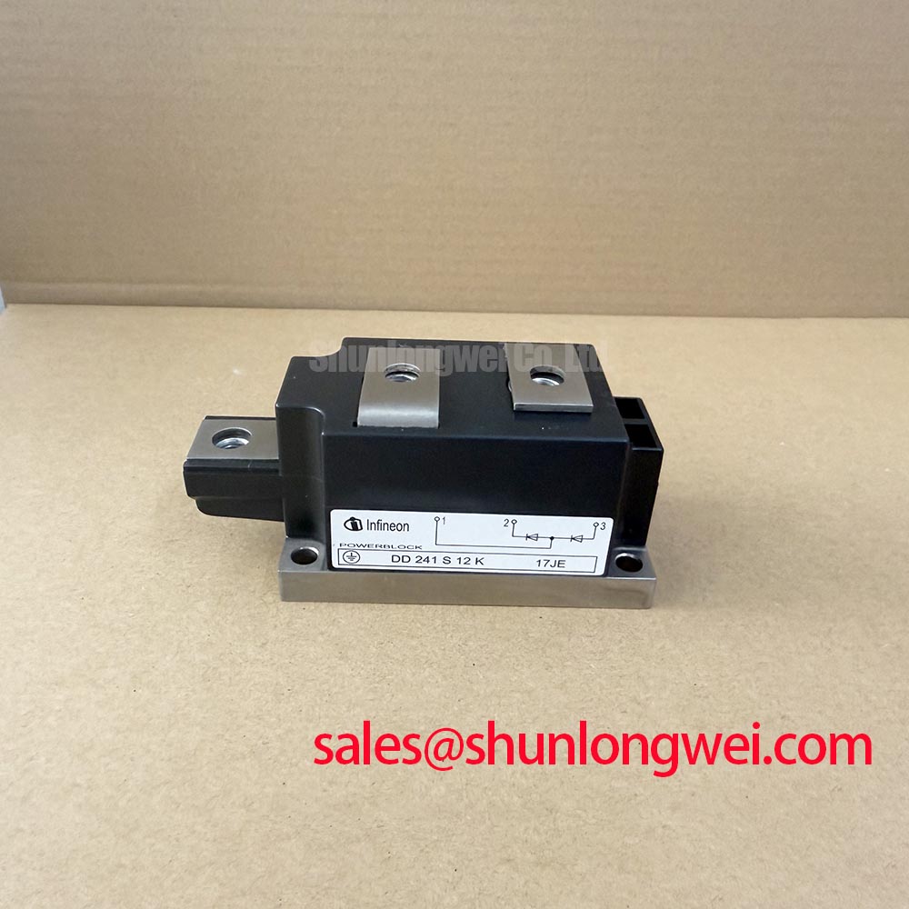
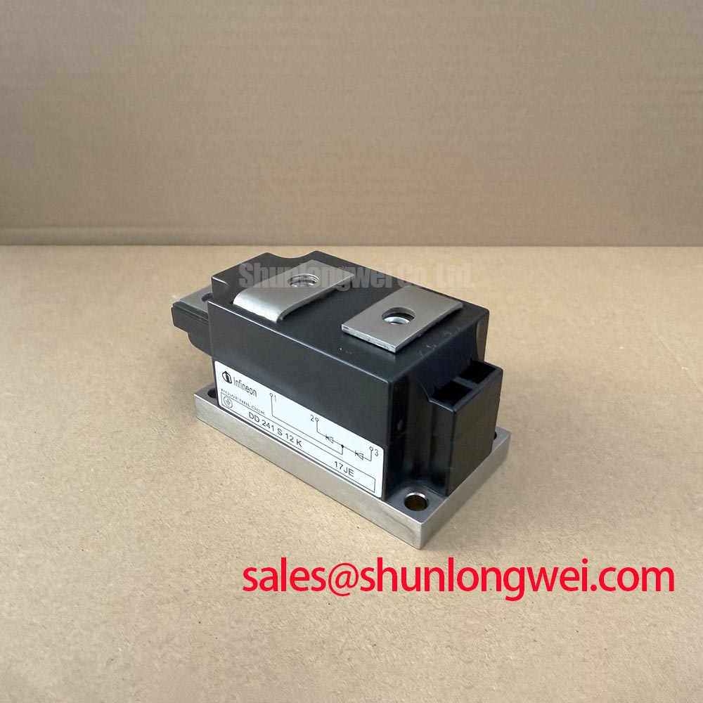
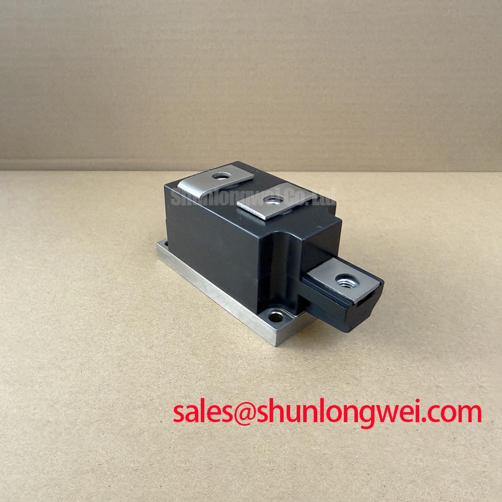
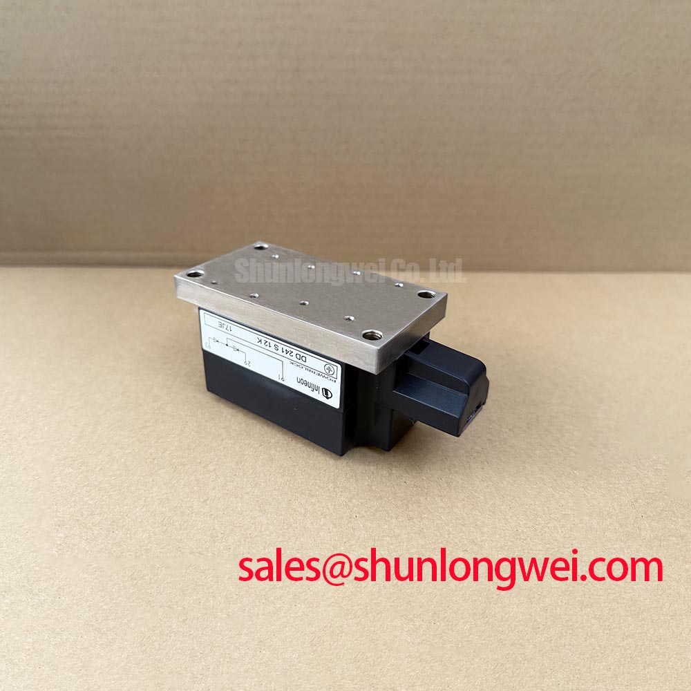
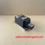
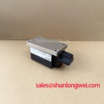
Begin incoming inspection by isolating the power circuit, identifying every module terminal from the original equipment drawing, and checking diode polarity with a multimeter in diode-test mode before reconnecting any busbar. The DD241S12 is an Infineon PowerBlock Module rated at 1200 V and 240 A as an Official Datasheet Specification. These three values define the verified electrical identity available for this product record and should be matched against the removed module and the equipment documentation before installation.
In a grid-tied static var compensator or thyristor-switched capacitor assembly, a diode module can appear in rectifier, freewheel, bypass, clamp, or auxiliary DC-link paths. The DD241S12 itself is a diode module, so it does not provide gate control, firing-angle control, or thyristor triggering. Any adjustment of firing delay angle is performed by the system’s thyristor controller and associated gate-drive circuitry. Engineers should therefore separate the control analysis from the diode-module verification process.
When reviewing AC-to-DC conversion at different firing angles, the useful field question is whether the DD241S12 is located in a path that sees changing average current, repeated commutation current, or transient reverse voltage. A lower firing angle can change the DC-side energy transfer and line-current waveform, while a larger firing angle can increase reactive-power demand in a controlled rectifier topology. The diode module must be evaluated against the actual circuit waveform, rather than against nominal output current alone.
The official 1200 V rating should be compared with the measured and documented repetitive blocking requirement at the module terminals. This review needs to include normal line variation, capacitor-bank switching events, transformer leakage effects, commutation overshoot, and any transient clamp behavior already present in the cabinet. The rating is not a statement that every system transient is automatically tolerated. It is the component’s specified voltage rating under the applicable conditions, and the system engineer should verify peak terminal voltage under representative operating and fault conditions.
The official 240 A current rating should likewise be treated as the module’s published current rating, not as a universal allowance for all pulsed, startup, commutation, or fault currents. In reactive-power compensation equipment, RMS current, crest factor, conduction interval, ambient temperature, heatsink performance, and load imbalance can all affect the electrical and thermal loading seen by a diode position.
During replacement work, compare the existing conductor arrangement with the original layout. A busbar that has been rotated, forced into place, or tightened while misaligned can create mechanical stress at the module terminals and can alter the current path. Design Consideration: keep the high-current loop compact where practical to reduce parasitic inductance that can contribute to turn-off and commutation overshoot. Final acceptance should come from system-level switching measurements and the original equipment electrical limits.
Where an adjacent rectifier or auxiliary power path is being reviewed at the same time, the TD210N12 can be assessed as a separate device record. It should not be treated as an automatic electrical substitute for the DD241S12 because device function, terminal arrangement, surge requirement, cooling interface, and circuit position must all be verified independently.
💡 Bench Tip: Record the cold diode-test direction and relative forward-reading behavior for each accessible terminal pair before removing a known-good assembly, then use that record only as a comparison reference after observing ESD-safe handling procedures.
Preventing Spurious Faults: AC Input Transient Overvoltage Clamping Guidelines for DD241S12
A diode-test check that shows unexpected conduction in both directions, no expected conduction in either direction, or results inconsistent with the original circuit diagram should stop the replacement process until the module is electrically isolated and the external network is checked. Parallel paths through capacitors, snubbers, thyristors, transformers, contactors, and measurement circuits can influence an in-circuit meter reading. A static diode check is useful for polarity confirmation, but it is not a complete proof of dynamic behavior under operating voltage and current.
AC transient protection should be reviewed as a complete network around the DD241S12, not as a property supplied by the diode module alone. Metal oxide varistors, RC snubbers, line reactors, surge arresters, capacitor-bank contact arrangements, and cable routing may all affect the voltage appearing across the module during switching events. The DD241S12 has a verified 1200 V rating, while MOV selection and RC snubber values are system-determined items that require the actual AC line condition, source impedance, protected topology, and measured transient waveform.
The commonly cited surge-immunity reference is IEC 61000-4-5. Its use in an equipment assessment does not mean that an individual diode module has independent system-level surge or EMC certification. Design Consideration: use the equipment’s applicable surge test plan, original protection architecture, and measured waveforms to determine whether the clamp network is limiting voltage at the diode terminals adequately during the relevant operating event.
For a thyristor-switched capacitor bank, contact bounce, capacitor energization, transformer switching, and commutation can create conditions that deserve separate waveform capture. A transient at the incoming AC terminals may not appear unchanged at the DD241S12 because intervening inductance, transformer coupling, clamp placement, and branch impedance reshape the event. Oscilloscope probing should follow safe high-voltage measurement practice and should compare the module-terminal waveform with the known equipment operating state.
Do not assign a generic MOV rating or an RC snubber component value to this specific module without the equipment schematic and validation data. Engineering Recommendation: preserve the original protection topology during urgent repair whenever possible, then investigate any changed waveform, damaged clamp component, loose connection, or altered busbar geometry before attributing a repeated fault to the diode module.
The manufacturer’s Infineon OptiMOS™ Low Voltage MOSFETs information is relevant as broader power-semiconductor context, but it does not define DD241S12 transient capability, diode behavior, or system protection values. Product-family data must not be transferred across unlike device technologies without a matching specification.
For equipment that has undergone substantial control-board or power-stage modification, technicians should verify whether the original transient suppression path is still present. A missing snubber lead, disconnected protective earth path, altered capacitor branch, or improperly seated busbar may produce symptoms that resemble a semiconductor failure while originating elsewhere in the power assembly.
Assembly Integrity and Layout Architecture: Baseplate Thermal Interface Review for DD241S12
Inspect the DD241S12 mounting face, heatsink surface, terminal hardware, insulating barriers, and busbar alignment before applying power. The supplied product information identifies the package as a PowerBlock Module, but it does not provide a verified thermal-resistance value, mounting-hole specification, mounting torque, terminal torque, heatsink flatness requirement, or thermal-interface thickness. These details must be taken from the original equipment documentation or the applicable manufacturer mechanical drawing rather than assumed from similar modules.
Baseplate contact quality matters because uneven contact pressure can create localized thermal stress even when the external heatsink appears clean. Design Consideration: use an appropriately prepared mating surface, apply the thermal interface material according to the original equipment procedure, and tighten mounting hardware in a balanced sequence so that the module is not distorted by one-sided loading. The final torque value must be determined by the documented hardware and module mechanical requirements.
Thermal resistance from junction to case, case to heatsink, and heatsink to ambient forms a series path, but no DD241S12 junction-to-case number should be inferred when it has not been provided in the official parameter set. The practical repair task is to inspect conditions that can worsen that path, including dried interface material, debris, corrosion, warped heatsink surfaces, missing fasteners, unequal clamping, blocked airflow, or an abnormal cooling circuit.
During a post-installation check, compare the repaired branch with an equivalent healthy branch where the equipment architecture permits. Thermal imaging, controlled load testing, current measurement, and inspection of terminal temperature trends can help reveal an imbalance. Such observations should be interpreted with circuit loading, sensor position, emissivity settings, airflow, and operating sequence in mind. A warmer location does not by itself prove that the diode module is defective.
The terminal layout should be reproduced from the original assembly. Avoid using terminal force to compensate for a busbar that does not naturally align. Current-sharing and transient behavior can be affected by conductor routing, loop area, joint cleanliness, and contact pressure. When replacing a module in a multi-device branch, inspect the companion devices and interconnects rather than assuming that the replaced position was the only stressed part of the event.
The Infineon Automotive Qualified Power Modules resource describes a separate qualified product context. It does not establish automotive qualification, thermal limits, insulation ratings, lifetime expectations, or environmental compliance for the DD241S12. Qualification claims must remain tied to the exact product documentation and the completed equipment assembly.
For broader repair planning, the Power Electronics Masterclass provides a useful reference point for reviewing voltage margin, cooling-path condition, and switching-test discipline. The DD241S12 should still be assessed from its confirmed 1200 V, 240 A, and PowerBlock identity together with the original system requirements.
Preventing Spurious Faults: I2t Sub-Cycle Melting Rating Guidelines for DD241S12
Before selecting or approving a semiconductor fuse for a branch containing the DD241S12, identify the exact fault path, upstream protective devices, available source energy, conductor impedance, transformer characteristics, capacitor discharge contribution, and the module’s documented surge and fault-current limits. The supplied official parameters confirm 1200 V, 240 A, and PowerBlock packaging, but they do not provide a DD241S12 fuse coordination table, I2t withstand value, non-repetitive surge-current value, or permitted clearing-energy limit.
For that reason, no numerical fuse I2t coordination value should be assigned to this module from general industry practice. A fuse’s pre-arcing I2t and total clearing I2t must be evaluated against the exact semiconductor withstand information supplied for the device and against the prospective current of the installed system. The objective is selective protection that removes a fault without allowing damaging energy to reach the semiconductor path, but the final coordination decision belongs to the equipment protection study.
In thyristor-switched capacitor and SVC assemblies, fault energy can be influenced by multiple sources. The AC supply, charged capacitor banks, DC auxiliary circuits, and magnetically stored energy may contribute differently depending on the instant of failure and switching state. A fuse that appears suitable from nominal current alone may not provide the desired behavior under a short-circuit event. Engineering Recommendation: retain the original fuse class and coordination approach unless a qualified system review confirms a change.
Inspection after a protective event should include the fuse body, fuseholder contacts, busbar joints, clamp network, capacitor branch condition, control interlocks, and all parallel semiconductor positions. Discoloration, mechanical movement, loose hardware, or altered conductor geometry can provide useful evidence, but none should be used as a single-cause diagnosis. Verify continuity, isolation, expected diode polarity, and control permissives against the equipment documentation before returning the branch to service.
When a cross-model comparison is necessary for procurement evaluation, DDB6U180N16RRP_B37 is a separate module listing that can be reviewed alongside the DD241S12. It is not a direct replacement declaration. Engineers should verify device function, voltage rating, current rating, package dimensions, terminal configuration, cooling interface, surge capability, fuse coordination, and the original circuit requirements before considering any substitution.
For the DD241S12 installation record, retain the module part number, measured terminal-polarity observations, original fuse identification, torque documentation from the equipment procedure, thermal-interface condition, and controlled commissioning results. This creates a practical reference for future service work without assigning unsupported lifetime, failure-rate, surge, insulation, or environmental-reliability claims to the module.