Content last revised on September 27, 2026
DD350N16K Diode Module Overview
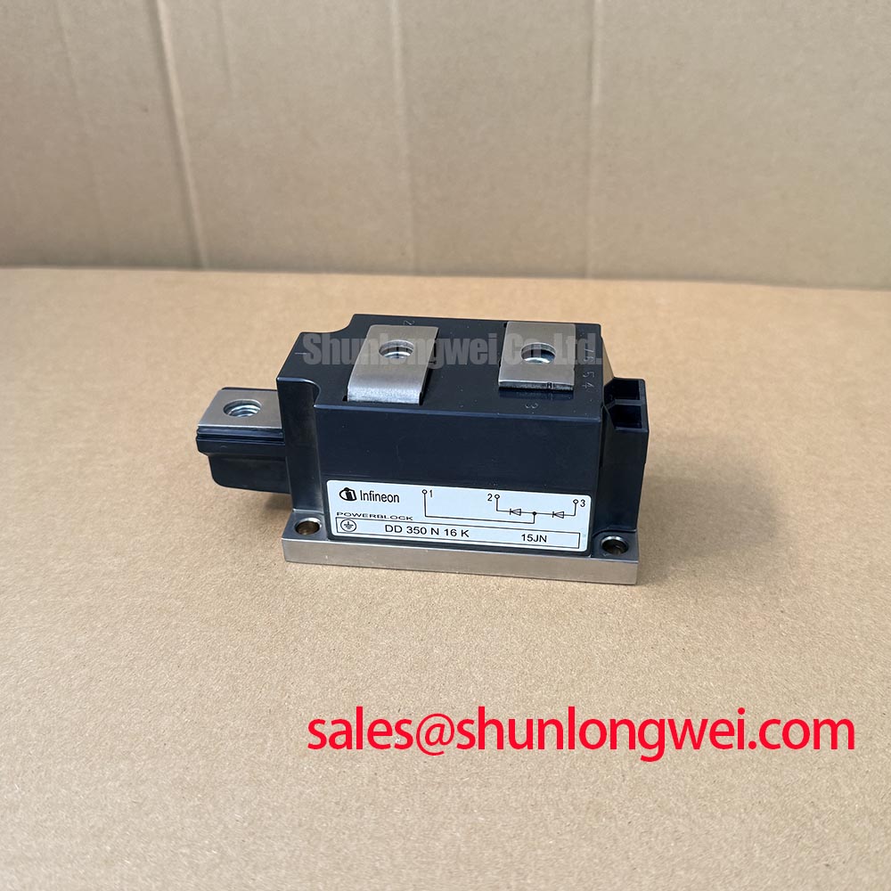
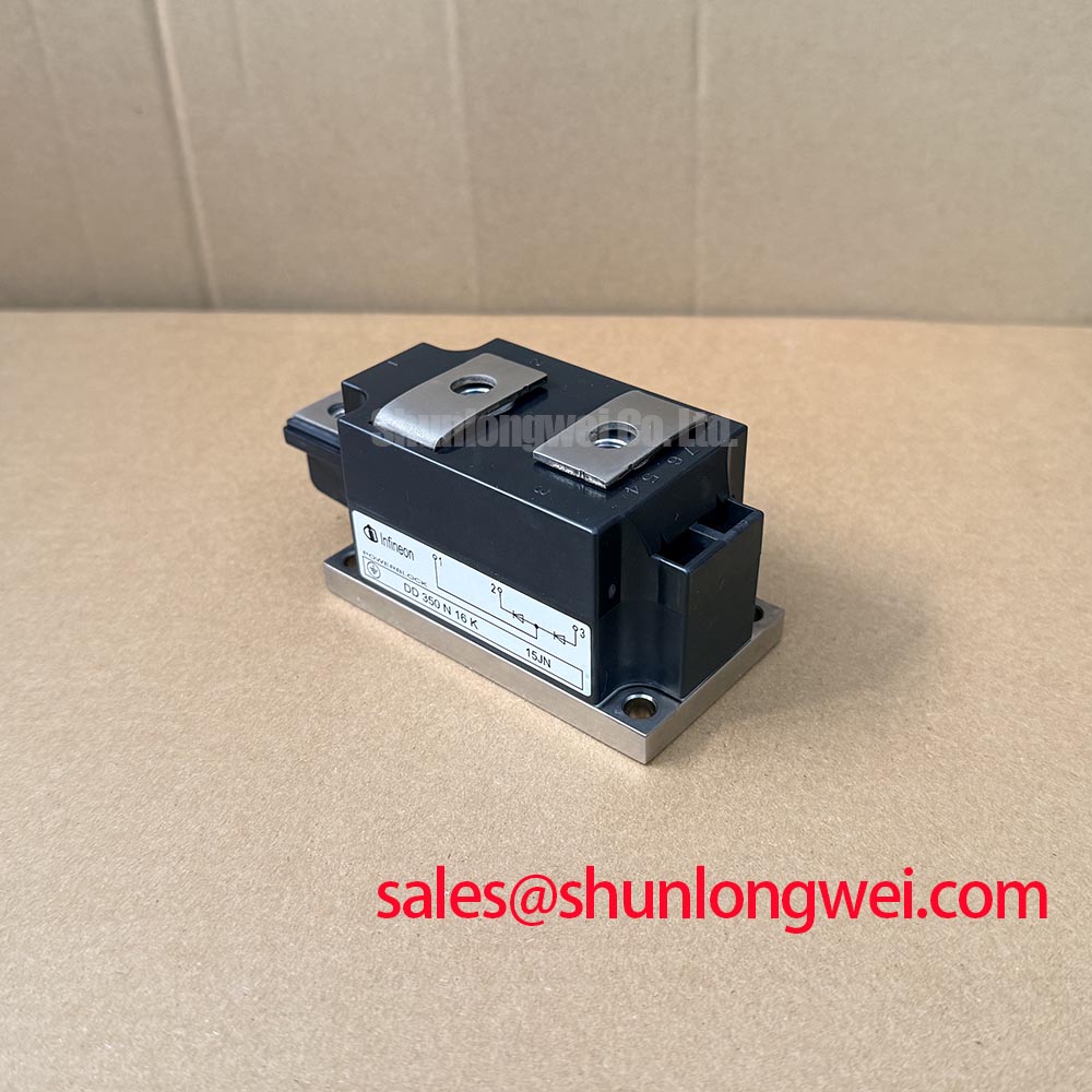
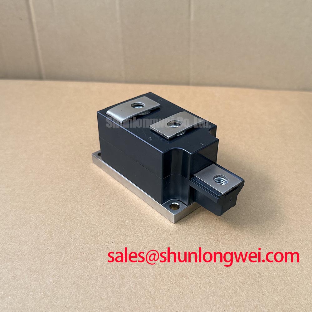
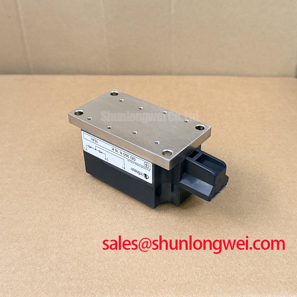
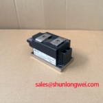
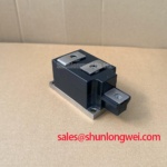
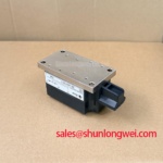
Verify the nameplate against DD350N16K, then confirm the cold-state terminal condition, baseplate flatness, and declared electrical boundary before connecting it to a live power assembly. The Infineon DD350N16K is a Diode Module in a PowerBlock Module package, with an official rated voltage of 1600.0 V and an official rated current of 350.0 A. These ratings identify the component class, but system engineers must still validate thermal, transient, fuse, and commutation conditions in the target circuit.
| Parameter | Official Specification |
|---|---|
| Manufacturer | Infineon |
| Part number | DD350N16K |
| Product category | Diode Module |
| Package | PowerBlock Module |
| Rated voltage | 1600.0 V |
| Rated current | 350.0 A |
Field Diagnostics & Commissioning: Baseplate Thermal Resistance in DD350N16K Topologies
For a grid tied static var compensator or thyristor switched capacitor assembly, begin commissioning with the mechanical heat path rather than applying full electrical stress. Inspect the module baseplate, heatsink mating surface, fastener condition, and thermal interface coverage. The product information supplied for this device does not establish a numerical Rth(j-c) value, so the applicable Infineon datasheet revision and the system thermal model must be checked before calculating junction temperature.
Uniform contact pressure is important because local lifting or uneven compression can increase thermal resistance even when the module appears electrically functional. Use the manufacturer’s specified mounting sequence and torque data for the actual package revision. Do not transfer a torque value from another PowerBlock module. A calibrated tool and a crosswise tightening sequence are appropriate design considerations, while the final torque remains a manufacturer and assembly documentation requirement.
Thermal paste should form a continuous, controlled interface without contaminating terminals or creating mechanical distortion. After assembly, inspect for movement at the baseplate and confirm that the heatsink remains aligned. Temperature measurements during a controlled current test should be compared with the expected semiconductor losses and cooling performance. An abnormal temperature gradient may require checking paste distribution, clamping uniformity, airflow, busbar heating, and the measurement attachment rather than assigning a single cause.
Terminal connections deserve the same verification. Confirm conductor preparation, contact surface cleanliness, connection hardware, and the terminal arrangement shown in the applicable technical drawing. Measure the voltage drop across the high current path during a controlled test and compare it with a known-good assembly when available. The 1600.0 V voltage rating and 350.0 A current rating are official product specifications, not a complete permission to operate at those values under every switching, ambient, or cooling condition.
Assembly Integrity & Layout Architecture: Implementing Saturable Reactor and Snubber Sizing to Protect DD350N16K
In an SVC or thyristor-switched capacitor topology, the diode module shares the commutation environment with bus inductance, capacitor banks, reactor elements, and surge suppression components. RC snubber selection should therefore be based on measured switching waveforms, capacitor characteristics, damping requirements, and the actual wiring geometry. The supplied product data does not provide an approved universal pair of snubber resistance and capacitance values for every installation.
A saturable reactor can influence the current rise profile and fault energy, but its suitability depends on the system topology and the magnetic component’s own operating limits. Designers should evaluate the reactor and snubber as a coordinated network. The bench verification should capture voltage overshoot, current rise, repetitive ringing, and temperature under the intended switching sequence. Minimize the commutation loop area to reduce parasitic inductance, then verify peak voltage against the module’s rated boundary during switching tests.
Gate-drive language should not be applied to this diode module as if it were a controllable IGBT or thyristor gate device. Any nearby controlled semiconductor requires its own driver reference, return path, and protection strategy. A negative turn-off bias, common-mode shielding, or bootstrap supply arrangement belongs to the associated controlled switch and must be validated from that device’s documentation. The DD350N16K page should not be used to infer an unlisted gate voltage, recovery specification, or control terminal function.
💡 Pro Tip: Keep the power and commutation conductors physically symmetrical where practical, then confirm overshoot and ringing with a properly rated differential probe before approving the assembly for full-voltage operation.
DD350N16K Operational Boundaries: Evaluating I2t Sub-Cycle Melting Rating Limits
Short-circuit protection requires coordination between the semiconductor’s permissible surge energy and the selected semiconductor fuse. The correct comparison uses the fuse manufacturer’s clearing I2t, prospective fault current, pre-arcing behavior, and the diode module’s official surge withstand data for the relevant pulse duration. No fuse I2t value is provided in the supplied product parameters, so a numerical coordination claim would be inappropriate without the applicable datasheets and fault study.
For a dead-short assessment, document the source impedance, DC-link or AC system voltage, protective device location, cable inductance, current sharing, and fault interruption time. Review whether the fuse is positioned to limit energy in the module rather than only clearing a downstream branch. The evaluation should also consider repetitive fault exposure, capacitor discharge contribution, and the possibility that parallel paths alter the current distribution.
During maintenance, isolate the assembly and discharge capacitors according to the equipment procedure before checking continuity or insulation condition. A low-resistance reading across a diode path cannot by itself establish safe operating condition; polarity, measurement current, parallel circuit paths, and temperature can influence the result. Compare the measured behavior with a documented known-good unit and inspect the module, fuse, busbar, and terminals together.
For broader troubleshooting methods covering power semiconductor measurements and failure analysis, consult the Field Engineer’s Handbook. It can support a structured inspection record without replacing the Infineon documentation for the DD350N16K.
DD350N16K Operational Boundaries: Evaluating Diode Peak Reverse Recovery Current and Soft Recovery Limits
Reverse recovery behavior affects commutation loss, voltage overshoot, acoustic noise, and radiated interference in high voltage capacitor switching equipment. The important parameters include reverse recovery peak current, recovery time, recovery softness, junction temperature, forward current, and applied commutation rate. These values are not included in the supplied official parameter set, so engineers should obtain the correct Infineon electrical characteristics before selecting snubber or reactor values.
Use a controlled double-pulse or equivalent commutation test only with a measurement setup rated for the circuit voltage and current. Capture the diode current and voltage simultaneously, using a low-inductance measurement path and a probe arrangement that does not create an unsafe ground connection. Compare the measured recovery waveform with the manufacturer’s test conditions because a value measured at one current and temperature cannot be transferred directly to a different SVC operating point.
Soft recovery is a system-level concern rather than a standalone label. A harder recovery transition can increase stray-inductance voltage excursion, while excessive damping can increase losses or alter the switching sequence. Designers should tune the surrounding network from measured waveforms and thermal results, then verify repetitive peak voltage, current sharing, and electromagnetic behavior against the applicable design limits.
For engineers assessing related high-power semiconductor technology, Infineon’s Automotive Qualified IGBTs provides useful manufacturer context, but it does not establish specifications for the DD350N16K. When a form-fit or circuit-level alternative is under review, the DDB6U180N16RRP_B37 should be evaluated independently against voltage, current, package, thermal, terminal, and protection requirements rather than treated as an automatic replacement.