


Content last revised on October 15, 2026
Transient Dynamics & Electrical Design: Preventing Electrical Overstress on DESI2X61-06C
I first trace the anode and cathode connections against the equipment schematic, because the DESI2X61-06C is a dual diode module, not a gate-controlled thyristor. Gate firing rise time, back-porch holding current, and multi-pulse triggering therefore do not describe its operation. A fault investigation should instead examine forward-current stress, reverse-voltage exposure, terminal continuity, and the switching conditions imposed by adjacent controlled devices.
The 600.0 V voltage rating and 60.0 A current rating are official product specifications. They are separate electrical limits, not evidence that every operating condition combining those values is permissible. As a Design Consideration, the engineer should relate measured operating waveforms to the applicable rating definitions, case temperature, and conduction duty before accepting the module for continuous service.
For surge protection coordination, compare the protective fuse’s total clearing I²t with the diode’s specified withstand data under corresponding pulse and temperature conditions. Continuous current alone cannot establish a suitable fuse. A short-circuit interruption assessment also needs prospective fault current and circuit voltage; selecting a fuse only from its nominal amperage overlooks the energy delivered before interruption.
Likewise, a nonrepetitive surge-current rating does not authorize repeated overloads. As a Design Consideration, evaluate the complete overload sequence and the thermal recovery between events rather than assigning an arbitrary recovery interval. After a protective trip, inspect the surrounding switching circuit and load before treating replacement of the diode module as the complete repair.
For replacement assessment, compare terminal topology, polarity, package drawing, electrical ratings, and switching characteristics. The RM100HA-20F provides another product reference for that comparison, but it should not be treated as a verified direct replacement for this IXYS module without a documented compatibility assessment.
DESI2X61-06C Thermal-Electrical Optimization: Dynamic Voltage Sharing and RC Damping in Practical Tuning
Capture reverse-voltage overshoot at the module terminals during the relevant switching transition, using probing suitable for the circuit voltage and measurement bandwidth. For this diode module, the immediate questions are reverse-recovery interaction, parasitic ringing, and peak reverse stress—not spurious gate turn-on. Triggering and Miller-effect checks belong to any associated controlled semiconductor, not to the diode itself.
As a Design Consideration, an RC damping network can be evaluated where measured ringing reveals an underdamped commutation path. Its resistance and capacitance should follow the observed oscillation, repetitive energy, and acceptable dissipation. A series reactor likewise requires system-level assessment of current slew, magnetic behavior, and losses; neither measure has a universal component value derived from the module’s headline ratings.
Pro Tip: Keep the commutation path compact and geometrically balanced, then verify reverse-voltage peaks at the module terminals under representative load transitions.
Voltage sharing becomes a separate assessment if a circuit places devices in series. Designers should distinguish static leakage-related sharing from transient sharing during commutation and evaluate the complete arrangement rather than assuming identical part numbers guarantee equal voltage distribution. The 600.0 V rating does not establish suitability for direct connection to a higher-voltage network.
When considering auxiliary power circuitry within a grid-tied static var compensator or thyristor-switched capacitor cabinet, verify the diode’s actual circuit role and electrical exposure. This is a compatibility assessment, not a claim that the module replaces the installation’s thyristor valve. For protection terminology, Transient-Voltage-Suppression Diodes for Surge Protection explains a distinct device function; a power rectifier should not be assumed to provide TVS clamping behavior.
Thermal & Mechanical Design: Junction-to-Heatsink Heat Dissipation on DESI2X61-06C
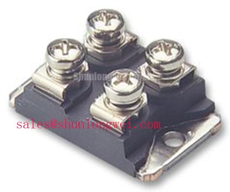
Inspect heatsink flatness, mounting surfaces, and terminal alignment before tightening the SOT-227B / TO-240AA package into place. As an Engineering Recommendation, busbars should meet the terminals without forcing the housing into alignment. Mechanical loading from a poorly fitted conductor can compromise an otherwise careful mounting operation.
Separate junction-to-case thermal resistance from the case-to-heatsink interface when reviewing heat flow. The former is a device characteristic; the latter depends on the assembled contact surfaces and interface material. Apply the specified assembly procedure and fastening torque rather than importing values from another package. Neither a copper baseplate nor double-sided cooling should be assumed from the package designation.
As a Design Consideration, inspect interface coverage and seating after assembly trials, then compare thermal behavior under matched operating conditions. Uneven heating can justify checking current distribution, terminal resistance, interface contact, and neighboring heat sources; it does not identify a single failure mechanism by itself. Press-pack spring-force calibration is not an appropriate substitute for the mounting requirements of this package.
For repeatable repair records, document terminal connections, protection changes, mounting conditions, and measured electrical and thermal behavior. The Field Engineer’s Handbook offers supporting troubleshooting context. Restore service only after the repaired assembly’s protection response and temperature behavior have been assessed under its intended operating conditions.

