


Content last revised on September 4, 2026
Field Diagnostics & Commissioning: High-Speed Fault Management: VCE Desaturation in DIM2400ESM17-PT500 Topologies
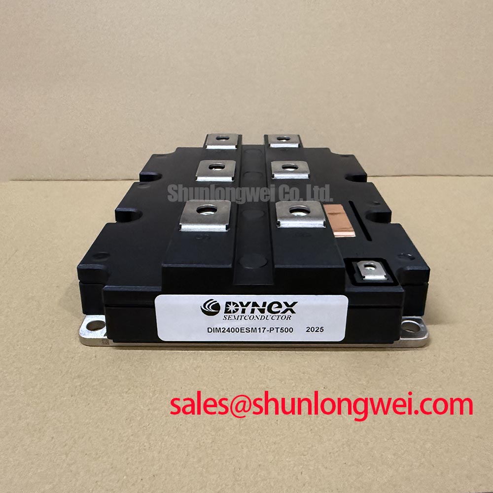
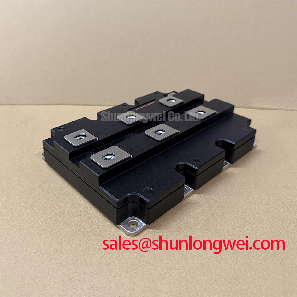
Before connecting the gate drive, verify the nameplate electrical boundary and inspect the module terminals, case interface, busbar contact faces, and cooling path for contamination, corrosion, looseness, or evidence of overheating. The DIM2400ESM17-PT500 is a DYNEX high-current IGBT module rated at VCES = 1700 V, with a continuous DC collector current of 2400 A at TC = 80 °C and a repetitive peak collector current of 4800 A, all Official Datasheet Specifications. Its specified operating junction-temperature range is −40 °C to +150 °C.
| Parameter | Specification | Classification |
|---|---|---|
| Collector-emitter voltage rating | 1700 V | Official Datasheet Specification |
| Continuous collector current at case temperature | 2400 A at 80 °C | Official Datasheet Specification |
| Repetitive peak collector current | 4800 A | Official Datasheet Specification |
| Gate-emitter permissible voltage | ±20 V | Official Datasheet Specification |
| Junction-to-case thermal resistance | 0.009 °C/W per switch | Official Datasheet Specification |
| Total switching energy per pulse | 1100 mJ at 2400 A, typical | Official Datasheet Specification |
| Operating junction-temperature range | −40 °C to +150 °C | Official Datasheet Specification |
Commissioning should begin with the protection path isolated from the power stage where the system architecture permits. Confirm that the desaturation sensing network, gate-driver supply, gate return, and fault output are correctly referenced before applying the intended DC-link voltage. A desaturation circuit monitors collector-emitter voltage while the IGBT is commanded on. A rising on-state VCE can indicate that the current has exceeded the usable operating condition, that a short-circuit event is developing, or that the gate drive is not establishing the intended enhancement state.
The module’s ±20 V VGES limit is an Official Datasheet Specification, not a prescribed drive voltage. The system integrator should verify the intended gate-drive levels, timing, desaturation blanking behavior, and protection thresholds against the original converter design and the applicable DYNEX documentation. The supplied module information does not establish a specific short-circuit withstand time or a mandatory protection response interval, so no fixed microsecond setting should be assumed for this part number.
Type I and Type II short-circuit conditions are often discussed in IGBT gate-driver design because the device can experience materially different electrical stress when a fault occurs during turn-on versus when it is already conducting. The practical maintenance task is to capture gate-emitter voltage, collector-emitter voltage, and current with measurement equipment suited to the converter’s energy level. Compare the waveforms with a known-good phase leg or approved commissioning traces. An irregular VCE rise can point to several conditions, including an overloaded phase, a gate-loop issue, an incorrect protection threshold, or abnormal commutation behavior. It should not be assigned to one cause without waveform evidence.
Two-stage soft turn-off is a Design Consideration for limiting the abrupt current interruption that can otherwise create substantial stray-inductance voltage. During a verified fault, the gate driver can first reduce current under controlled conditions and then complete turn-off, subject to the converter’s validated safe-operating-area strategy. This is particularly relevant where the module handles high current and the DC bus contains distributed inductance. The resulting peak collector-emitter voltage must be verified during switching tests against the system DC-link voltage and the 1700 V device rating.
⚠️ Maintenance Note: Periodically monitor terminal contact temperature rise and confirm that heatsink airflow paths remain clear before a high-current traction inverter is returned to service.
For equipment repair teams comparing current capability and voltage class across different converter positions, the linked FF45017ME4 provides a separate reference point that should be evaluated only against the original electrical, mechanical, and gate-drive requirements.
DIM2400ESM17-PT500 Circuit Protection & Reliability: Calibrating High-Frequency Commutation Loop Inductance
The physical DC-link commutation loop deserves inspection whenever the DIM2400ESM17-PT500 is installed or replaced. In practical terms, switching overshoot follows the relationship between DC-link voltage, stray loop inductance, and the rate of current change: Vpeak rises above the DC-link level by the inductive term Lσ multiplied by di/dt. This is an Engineering Calculation principle rather than an individual module guarantee. The busbar, DC-link capacitor placement, device terminal arrangement, and switching conditions determine the result.
A stray commutation-loop inductance target of less than 25 nH is a Design Consideration for busbar layout supplied for this application context. It should be treated as a layout objective to suppress turn-off overshoot, not as an official mechanical specification of the IGBT module. A compact laminated or symmetrical planar busbar arrangement can reduce loop area, while the final design must be verified through measured switching waveforms under representative current and temperature conditions.
The 1100 mJ total switching energy per pulse at 2400 A is an Official Datasheet Specification stated as typical. It informs thermal and switching-loss assessment, but it does not alone establish converter power capability, permissible repetition rate, or heatsink selection. Those outcomes depend on the operating waveform, modulation strategy, cooling assembly, ambient conditions, gate-drive behavior, and actual current duty.
Freewheeling-diode reverse recovery can influence voltage overshoot and radiated emissions because reverse-recovery current interacts with the same commutation inductance. A sharp recovery transition may produce ringing that appears across the device, DC-link terminals, and nearby measurement points. Snubber capacitors and related damping networks are Engineering Recommendations that require system-specific selection. Their capacitance, placement, damping method, and voltage rating should be validated from captured commutation waveforms rather than copied from an unrelated inverter.
Where a power stage contains an upstream rectifier or an associated complementary switching function, an item such as BSM75GD120DLC can be reviewed as a separate system component. Electrical compatibility must be established from the actual topology, voltage class, current demand, mounting arrangement, and protection coordination.
Avalanche behavior is associated with breakdown under excessive reverse electrical stress. The physical mechanism is outlined in Avalanche Breakdown in High Voltage Power Semiconductors. The 1700 V VCES specification defines the module’s stated blocking-voltage rating; it does not authorize uncontrolled repetitive overvoltage operation. When abnormal peaks are observed, inspect the busbar loop, capacitor connections, snubber condition, and gate-drive turn-off behavior before returning the equipment to duty.
Preventing Spurious Faults: Symmetrical Busbar Geometry for High-Current DIM2400ESM17-PT500 Installations
At 2400 A continuous current at TC = 80 °C, terminal symmetry is a practical reliability issue. Parallel conductors with unequal length, contact area, or return geometry can develop different impedance and inductive behavior. This can distort current sharing and cause one path to exhibit a higher transient voltage or local temperature rise than adjacent paths. Before commissioning, inspect every high-current interface for aligned contact surfaces, appropriate hardware engagement, and a clean, stable thermal path.
The positive temperature coefficient of IGBT on-state behavior is often considered helpful for steady-state current sharing in parallel arrangements. That observation is a Design Consideration, not proof that any parallel implementation will share safely. Dynamic sharing is affected by gate-loop impedance, device variation, busbar symmetry, temperature distribution, switching timing, and driver behavior. A parallel installation therefore requires phase-current and switching-waveform verification under the actual converter conditions.
Spurious protection events should be investigated with synchronized measurements rather than reset repeatedly. Check whether the fault signal coincides with a genuine VCE increase, gate-voltage disturbance, DC-link transient, current-sensor anomaly, or control-supply interruption. Condensation, conductive dust, aged thermal material, and loose terminal hardware can each contribute to unstable operation without producing the same visible symptom every time. In forklift and material-handling traction systems, vibration and repeated thermal cycling make routine fastening inspection and cooling-system cleaning especially relevant.
The published 0.009 °C/W junction-to-case thermal resistance per switch is an Official Datasheet Specification. It describes one part of the heat path only. Heatsink flatness, interface material condition, mounting pressure, fan performance, enclosure airflow, and ambient temperature remain system-dependent factors. Design Consideration calls for inspecting thermal interface material during planned maintenance and replacing it when its condition no longer supports uniform contact.
Engineers reviewing long-term power-conversion technology options can also consult The 1200 V CoolSiC™ MOSFET Advantage in Three. That resource concerns a different technology and voltage class, so it should not be interpreted as a direct substitute or performance claim for the DIM2400ESM17-PT500.
Transient Dynamics & Electrical Design: Optimizing Gate Drive Loop Geometry to Prevent Oscillation on DIM2400ESM17-PT500
Gate-drive wiring should be examined as a measurement and control loop, not as an incidental harness. The gate path must have a controlled return reference so that high main-current emitter voltage does not unintentionally alter the voltage seen by the gate driver. Separating the low-current gate return from the main high-current emitter return is a Design Consideration intended to reduce mutual coupling and unwanted gate-voltage movement during switching.
During troubleshooting, observe gate-emitter voltage directly at the relevant module control terminals using an appropriate differential measurement method. Oscillation, delayed turn-off, or unexplained desaturation events may indicate excessive loop inductance, unsuitable probe placement, a compromised gate return, driver supply instability, or interaction with the power commutation loop. The corrective action should follow the observed waveform and validated converter design rather than a generic gate-resistor value.
The 4800 A repetitive peak collector-current rating is an Official Datasheet Specification, but it is not a blanket allowance for uncontrolled surge testing. Current stress must be assessed together with pulse duration, junction temperature, DC-link behavior, switching loss, and the applicable safe-operating-area information. If a commissioning trace shows unexpected overshoot or ringing, reduce test exposure and investigate the mechanical and electrical loop geometry before resuming full-load operation.
For electric material-handling and forklift low-voltage traction inverter assessments, the module’s high current rating can be relevant where the original architecture uses this device class. The installer should confirm the original power-stage topology, cooling interface, gate-driver configuration, protective interlocks, and busbar geometry before fitting a replacement unit. The specified −40 °C to +150 °C operating junction-temperature range supports evaluation across industrial temperature conditions, while enclosure sealing, moisture control, and thermal cycling remain responsibilities of the complete equipment design.