



Content last revised on October 21, 2026
Transient Dynamics & Electrical Design: Bi-Directional DC-DC Buck-Boost Conversion on DP50H1200T101757
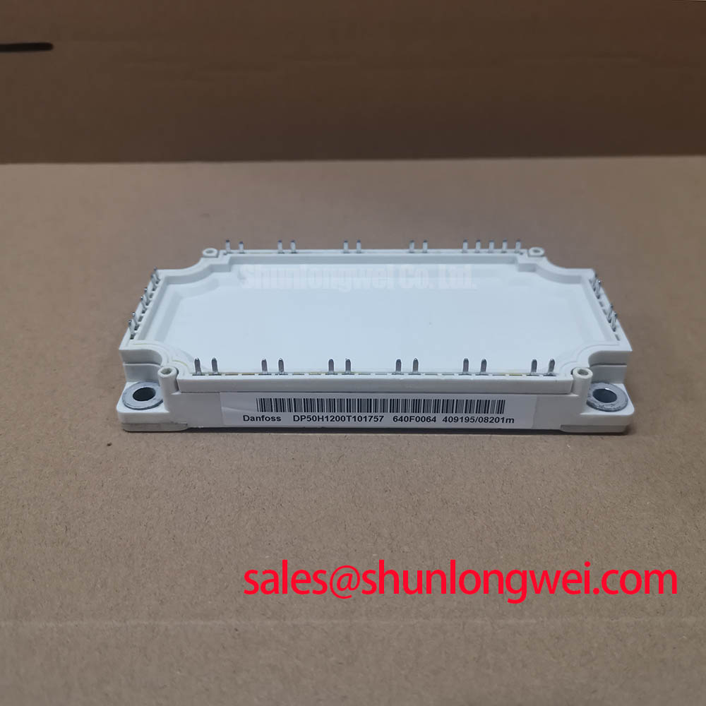
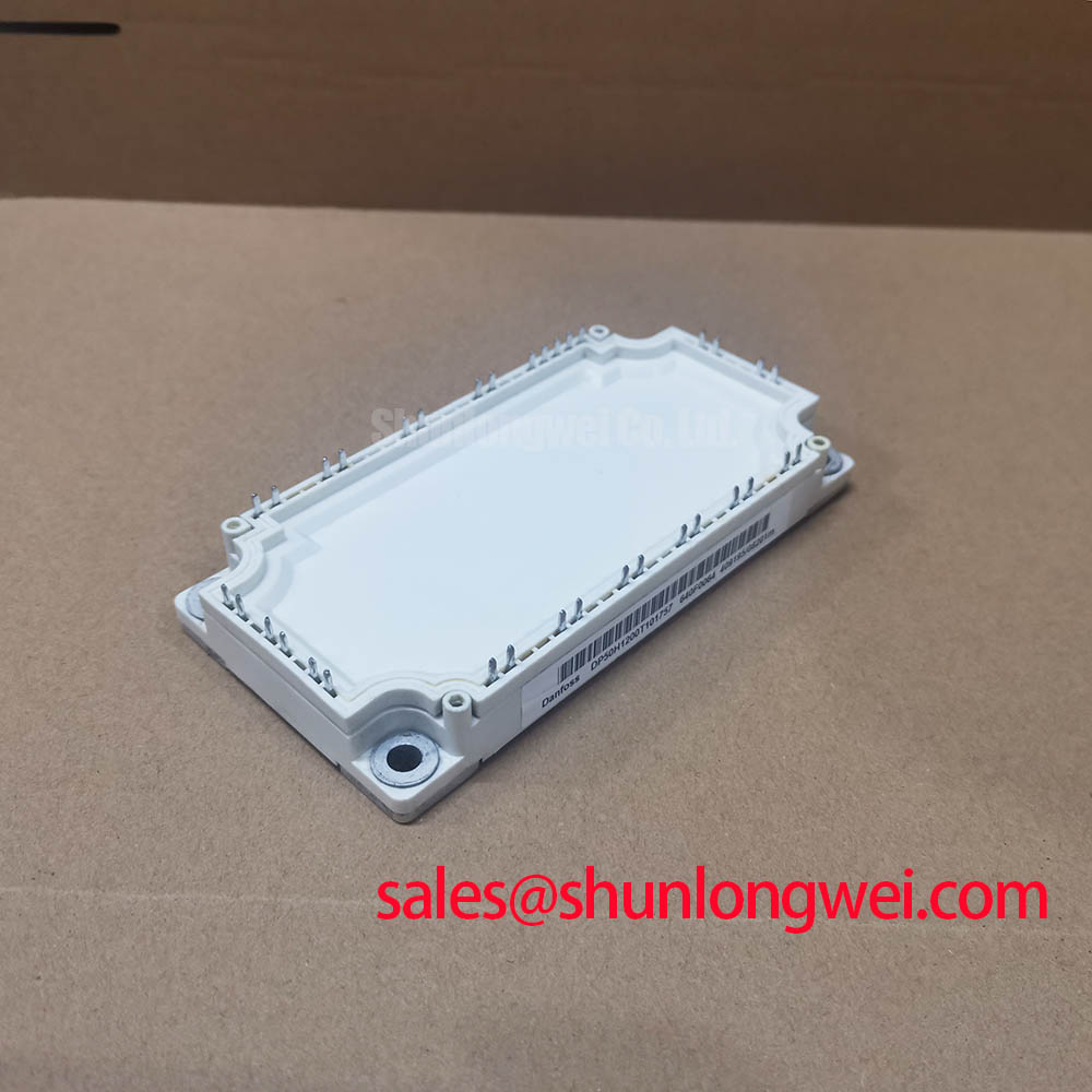
Isolate the DC supply, verify that stored energy has discharged, and compare the installed module marking with DP50H1200T101757 before disconnecting the power terminals. Record terminal positions, gate wiring, heatsink condition, and any localized discoloration so the repair preserves evidence of the original fault rather than simply replacing the power stage.
The Danfoss DP50H1200T101757 IGBT module has an Official Specification of 1200 V collector-emitter blocking voltage and 50 A continuous collector current at a case temperature of 100°C. Its integration assessment should connect those electrical boundaries with the actual cooling arrangement, switching behavior, and protection sequence.
Capture current direction, DC-link voltage, and switching transitions during both power-flow directions before changing gate-drive settings. As a Design Consideration, a stage that operates normally while charging can expose different commutation stresses during discharge because the conducting switches and freewheeling paths change roles. Compare equivalent operating points rather than treating unequal waveforms as immediate evidence of module damage.
For compatibility assessment, commercial string inverters and micro-grid energy-storage converters are potential equipment contexts, subject to their circuit topology, control strategy, and mechanical interfaces. Bidirectional battery power transfer does not by itself establish four-quadrant operation; the complete converter determines which voltage and current polarities are supported. The module rating alone does not establish that capability.
During repeated peak-shaving cycles, log case temperature alongside current and operating state. The Official Specification for operating junction temperature is −40°C to +150°C, which is a junction boundary rather than an ambient-temperature rating. Case measurements help identify changing cooling conditions, but estimating junction temperature also requires losses and the relevant thermal model.
The Official Specification for junction-to-case thermal resistance is 0.32 K/W per IGBT. The 390 W power-dissipation rating at a case temperature of 25°C is also an Official Specification, not a promise that the assembled converter can continuously remove that heat. As a Design Consideration, inspect heatsink airflow, interface condition, mounting flatness, and cooling-system performance before attributing thermal trips to semiconductor deterioration.
Keep commutation paths compact to limit inductive overshoot, with the final conductor arrangement established by switching measurements and the equipment insulation design. Check electrical clearances against working voltage, contamination conditions, and the applicable equipment requirements rather than imposing a generic spacing. Where a bootstrap driver is already used, assess its supply during the longest commanded conduction intervals; capacitor recharge and diode recovery belong to that driver assessment, not to the module’s published ratings.
DP50H1200T101757 Circuit Protection & Reliability: Calibrating Baseplate Isolation Breakdown Testing
Separate the module from connected gate electronics, sensing circuits, and other vulnerable equipment before applying any approved terminal-to-baseplate insulation test. As a Design Consideration, use the equipment service procedure and the module’s specified test configuration to select test voltage, duration, terminal grouping, and acceptance criteria. Insulation resistance measurement and dielectric withstand testing answer different questions and should not be treated as interchangeable procedures.
Clean and dry accessible insulating surfaces before interpreting an abnormal reading. Conductive dust, moisture, damaged external insulation, and connected circuitry can influence the result. A terminal-to-baseplate measurement alone cannot identify a particular internal substrate defect. Document the environmental condition and test arrangement so later measurements remain comparable.
The following comparison keeps the confirmed DP50H1200T101757 ratings separate from the evidence needed to assess another repair candidate. “Consult datasheet” identifies a procurement verification task, not an assumed match.
| Selection criterion | DP50H1200T101757 | MG50N2YS1 comparison requirement |
|---|---|---|
| Collector-emitter voltage | 1200 V — Official Specification | Consult datasheet |
| Continuous collector current | 50 A at case temperature 100°C — Official Specification | Compare rating and case-temperature condition |
| Short-circuit withstand time | 10 µs — Official Specification; specified test conditions apply | Compare withstand conditions and protection requirements |
| Power dissipation | 390 W at case temperature 25°C — Official Specification | Compare thermal boundary conditions and per-device rating definition |
| Junction-to-case thermal resistance | 0.32 K/W per IGBT — Official Specification | Compare per-device thermal definition |
| Operating junction temperature | −40°C to +150°C — Official Specification | Consult datasheet |
| Mechanical and circuit compatibility | Confirm terminal map, outline, and mounting requirements | Compare all interfaces before substitution |
When reviewing repair materials, the MG50N2YS1 can be included as a comparison candidate, not designated a direct replacement from its model name. Engineering Recommendation: reconcile internal circuit configuration, terminal assignments, gate characteristics, switching losses, and mounting interfaces before approving any substitution. A shared headline rating does not resolve those differences.
Thermal cycling also deserves attention during maintenance. The general principles of thermal expansion coefficient mismatch and the Coffin-Manson thermal fatigue model explain why repeated temperature excursions can stress assemblies; they do not establish a service-life prediction for this module. Set inspection intervals from equipment duty and temperature trends, including checks for condensation after cold shutdowns.
DP50H1200T101757 Circuit Protection & Reliability: Calibrating Active Miller Clamp Implementation
Measure gate-to-emitter voltage at the module connection during complementary-switch transitions to investigate suspected parasitic turn-on. As a Design Consideration, collector voltage transitions can couple displacement current through gate-collector capacitance. Whether that disturbance becomes unwanted conduction depends on the complete gate-return path, driver behavior, and operating conditions.
An active Miller clamp provides a low-impedance discharge path when engaged, but its effectiveness depends on activation timing and connection inductance. Inspect the physical clamp loop and shared return conductors before changing components. Compare the gate disturbance with collector current and switching-node voltage using appropriately rated probes; probe-loop pickup can otherwise resemble a genuine gate excursion.
Negative off-state bias is a system-level design option, not an established requirement for DP50H1200T101757. Engineering Recommendation: select any bias and clamp arrangement within the module and driver gate-voltage limits, then evaluate gate excursions during startup, shutdown, and fault response. Avoid copying settings from a different module simply because its voltage class appears similar.
Where switching topology is under review, Resonant Topologies in Home Appliances provides complementary background on how circuit architecture changes commutation behavior. It is topology context rather than evidence of this module’s suitability for a particular application. For an existing repair, preserve the validated control sequence unless the equipment engineering process authorizes a change.
Maintenance Note: Trend power-terminal temperature and inspect cooling airflow during scheduled service, using the specified tightening procedure rather than tightening connections by feel.
Preventing Spurious Faults: Coordination of High-Speed Arcing Voltage Guidelines for DP50H1200T101757
Compare the semiconductor fuse’s DC interruption characteristics with the actual link voltage, prospective fault current, and circuit time constant before accepting the protection arrangement. As a Design Consideration, the fuse’s arcing voltage contributes to the transient stress seen by the surrounding circuit. Its voltage rating alone does not describe the complete interruption event.
The module’s 10 µs short-circuit withstand time is an Official Specification under its applicable test conditions. It is not a fuse-clearing allowance or an assurance against enclosure rupture. Fast electronic detection and controlled gate shutdown address semiconductor fault exposure, while coordinated upstream protection limits continuing energy from the source.
Assess fuse total clearing I²t against documented withstand information for the protected current path, including conductors and interconnections. Short-circuit withstand time cannot be converted directly into a module I²t rating without the necessary current waveform and device limits. Protection acceptance therefore needs the equipment’s validated coordination method rather than a comparison of unrelated headline numbers.
For intermittent trips, preserve fault-recorder traces and compare protection timing with DC-link disturbances, driver supply behavior, and switching commands. Inspect fuse holders, power joints, and nearby insulation for heat or contamination without assuming that a single visible symptom identifies the initiating fault. After corrective work, verify the approved shutdown sequence and interruption arrangement under the equipment’s controlled test procedure before returning the power stage to service.