


Content last revised on September 14, 2026
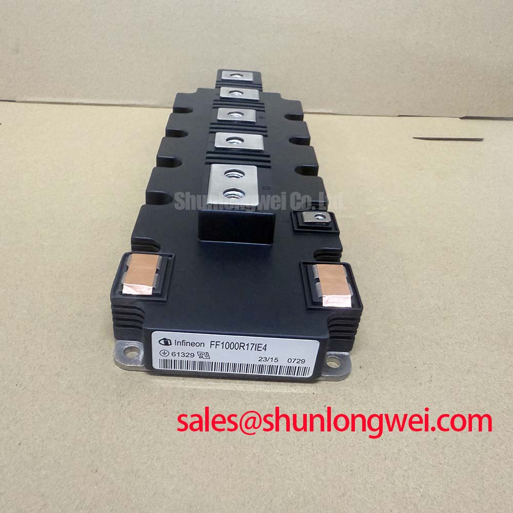
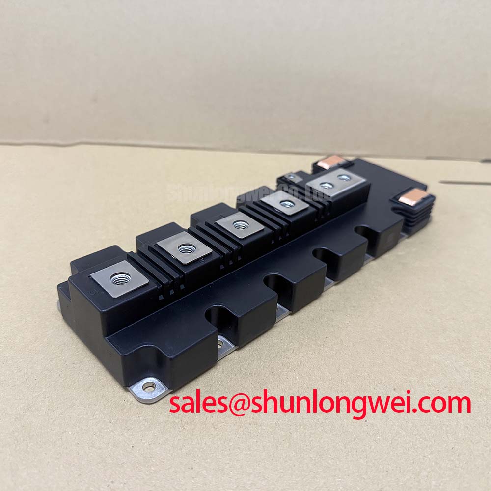
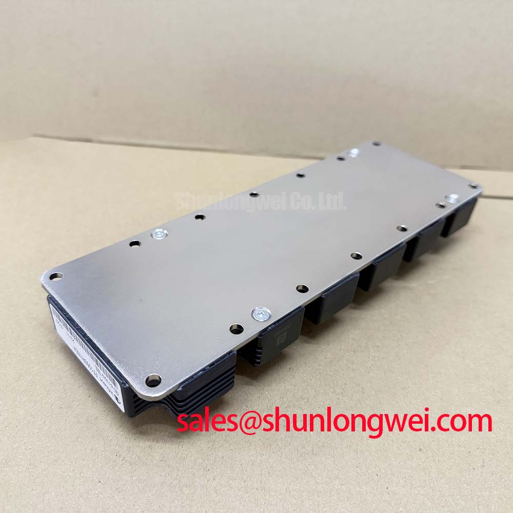
Infineon FF1000R17IE4 1700V 1000A IGBT Module for Utility Scale PCS
Before energizing a replacement unit, inspect the housing and terminals, confirm the nameplate against the system bill of materials, and verify the electrical boundary of FF1000R17IE4 against the original converter design. This Infineon IGBT module is specified with a 1700 V collector emitter voltage, a 1000 A rated DC collector current, and a maximum operating junction temperature of 150°C. These values support a structured compatibility review for high power industrial inverters and utility scale centralized battery energy storage power conversion systems.
The figures below are official specification values supplied for this product page. They should not be interpreted as a complete system design limit. Switching frequency, overload duration, gate drive conditions, cooling performance, DC link behavior, and current waveform remain system determined.
| Parameter | Official value | Engineering significance |
|---|---|---|
| Collector emitter voltage, VCES | 1700 V | Provides a high voltage blocking boundary for evaluating demanding inverter DC links, subject to switching transient verification. |
| Rated DC collector current, IC | 1000 A | Supports high power output in suitable dual switch converter arrangements when thermal and electrical conditions are validated. |
| Collector emitter saturation voltage, VCE(sat) | 2.00 V typical at Tvj = 125°C | Helps engineers estimate conduction loss during the specified test condition. Actual loss depends on current, duty cycle, temperature, and switching operation. |
| Isolation test voltage | 10.2 kV | Indicates the stated dielectric test capability. It is not a permission to operate the power circuit at the same voltage. |
| Maximum operating junction temperature, Tvj op | 150°C | Defines the listed junction temperature ceiling for thermal assessment and protection coordination. |
Transient Dynamics and Electrical Design: Thermal Time Constants and Peak Junction Temperature on FF1000R17IE4
During commissioning, measure the case temperature near the module mounting surface while recording phase current, DC link voltage, switching state, and cooling conditions. A single surface temperature reading cannot prove junction safety. The useful maintenance question is how quickly the junction responds to a pulsed load and how much heat remains in the case and heatsink when the pulse ends.
Thermal analysis is an Engineering Calculation, not an additional factory rating. A multi resistance and capacitance thermal model can represent the short time junction response, the case response, and the slower heatsink response. For a heavy pulse, engineers should calculate the junction temperature from the initial junction condition, the measured or specified power waveform, and the applicable transient thermal impedance data. If the exact transient thermal impedance curve is not available in the documentation used for the installation, the safe approach is to obtain the correct manufacturer data rather than substitute a generic curve.
The stated 150°C maximum operating junction temperature is the boundary to check during the calculation. The stated 2.00 V typical VCE(sat) at 125°C can be used as a reference point for conduction loss estimation, but it is not a fixed voltage across every operating condition. Current imbalance, modulation pattern, gate timing, junction temperature, and semiconductor tolerances can all change the real loss profile.
For a utility scale centralized battery energy storage PCS, the physical inspection should include the heatsink contact area, cooling channel condition, fan or liquid circuit operation, and signs of uneven thermal transfer. Designers should minimize the commutation loop area and keep high current paths mechanically stable so that stray inductance does not create excessive turn off overshoot. The resulting peak voltage must be verified with appropriate high bandwidth measurement equipment against the DC link voltage and the module voltage rating.
When evaluating high voltage IGBT technology across an industrial converter portfolio, engineers may also consult the Infineon IGBT Modules and Discretes Official Portfolio. That portfolio reference does not replace the product specific documentation required for this module.
Preventing Spurious Faults: High Altitude Cosmic Ray Induced SEB Failure Guidelines for FF1000R17IE4
Altitude and cosmic ray related reliability require a source based assessment. No FIT rate, single event burnout probability, or altitude derating value is stated in the supplied product parameters, so a numerical SEB prediction should not be assigned to FF1000R17IE4 from general assumptions. This is a Design Consideration requiring the manufacturer reliability data, the installation altitude, the DC link operating profile, and the system protection study.
At an elevated installation site, the engineering team should document the maximum DC link voltage, repetitive overshoot, dwell time at high voltage, switching energy, and protective shutdown behavior. The 1700 V VCES rating is the official blocking voltage specification, while the actual design margin depends on the complete commutation circuit. A bench test should capture the collector emitter waveform at the module terminals under the intended gate resistance, load current, temperature, and bus voltage.
Busbar geometry should be reviewed to reduce parasitic inductance in the power commutation path. This is a Design Consideration rather than a product specific dimensional rule. Engineers should place the appropriate snubber film capacitor close to the switching loop when the circuit analysis shows that it is required, then validate the capacitor current, pulse energy, insulation arrangement, and temperature rise. The final layout must be verified by measurement, not by assuming that a nominal busbar arrangement will produce the expected transient behavior.
High voltage clearance and creepage also need to be checked against the enclosure, contamination level, altitude, insulation system, and applicable equipment standard. The listed 10.2 kV isolation test voltage identifies the stated isolation test level; it does not independently certify the finished PCS for an EMC, safety, or insulation compliance claim. The complete assembly remains responsible for those evaluations.
For practical service planning, the reference article on Industrial Applications can be used alongside the converter manufacturer’s test procedure when reviewing renewable energy and heavy industrial operating conditions.
FF1000R17IE4 Thermal Electrical Optimization: Derating Guidelines and Mismatched Parameter Practical Tuning
The positive temperature behavior commonly associated with IGBT saturation voltage can assist static current sharing in parallel power paths, but it should not be treated as proof of dynamic current balance. The supplied product information confirms the typical 2.00 V VCE(sat) at 125°C; it does not provide a guaranteed current sharing tolerance, parallel operation rule, gate loop specification, or thermal resistance value.
When several switching paths operate within one converter, keep the gate wiring symmetrical and verify the return path, gate resistor arrangement, driver propagation delay, and local decoupling. These are Engineering Recommendations for reducing timing mismatch. The correct values remain system determined and should be established through double pulse testing, current probe comparison, and collector emitter voltage measurement under the intended temperature range.
A mismatch between two paths may appear as unequal switching loss, uneven case temperature, different turn on delay, or an abnormal voltage transient. None of these symptoms identifies one cause by itself. Inspect the gate waveform at the module terminals, compare the power loop impedance, check driver supply stability, and confirm that the thermal interface has consistent contact. The 1000 A rated DC collector current should not be divided mechanically between parallel devices without reviewing the actual waveform and cooling capability.
Derating is a Design Consideration based on the complete operating envelope. Engineers should account for ambient temperature, heatsink temperature, airflow or coolant condition, overload profile, switching loss, conduction loss, and fault response. A numerical derating percentage cannot be stated responsibly without the relevant thermal curves and duty cycle. The junction calculation should use the measured power waveform and confirm that the predicted peak remains below the official 150°C maximum operating junction temperature.
For replacement planning, the electrically compatible role of another product must be confirmed from its own data. A neutral comparison point for service teams is FF45017ME4, but voltage class, current capability, mechanical dimensions, gate characteristics, isolation construction, and driver compatibility must be checked before any substitution is considered.
Field Diagnostics and Commissioning: DC DC Converter Interleaving and Ripple Current in FF1000R17IE4 Topologies
Commissioning should begin with the DC link isolated and discharged, followed by inspection of busbar joints, gate driver connectors, auxiliary supplies, and the cooling system. In a bidirectional battery energy storage PCS, power can move from the battery racks to the inverter link or in the reverse direction. Each direction changes switching states and thermal distribution, so testing only one power flow does not establish complete operating compatibility.
For an interleaved DC DC stage, compare the phase current waveforms and switching node behavior at controlled load points. Ripple current can increase capacitor heating and create additional semiconductor switching stress, while imperfect phase timing can produce unequal thermal loading. Designers should verify the control sequence, dead time, current sensor polarity, and gate driver timing against the approved system schematic. The module’s 1700 V collector emitter rating and 1000 A rated DC collector current remain component specifications, not a substitute for converter level ripple and overload validation.
Thermal cycling during peak shaving should be evaluated with synchronized electrical and thermal records. Monitor case temperature, cooling inlet and outlet conditions, phase current, DC link ripple, and fault timestamps. A temperature rise may reflect electrical loss, impaired thermal contact, restricted airflow, coolant problems, or control imbalance; further measurement is needed before assigning a single fault cause.
The front end of the PCS may include a rectifier or another active power conversion stage whose switching behavior interacts with the IGBT bridge. Engineers reviewing the complete topology can reference FZ3600R12HP4 as a related system level component, while confirming all voltage, current, trigger, timing, and protection requirements from the respective documentation.
⚠️ Maintenance Note: Clean the heatsink and cooling path at the scheduled service interval, inspect thermal interface aging, and recheck terminal tightness using the equipment manufacturer’s approved procedure before returning the PCS to load.