Content last revised on October 15, 2026
FF1200R17KE3_B2 Operational Boundaries: Evaluating Thermal Time Constants and Peak Junction Limits
- Record cold unpowered resistance and diode readings across the main power terminals and antiparallel diode path.
- Inspect the module seating plane, heatsink contact, thermal interface condition, and terminal hardware before applying DC power.
- Check gate driver isolation, gate return continuity, clamp operation, and the physical separation of power and control wiring.
- Confirm that the installed assembly matches the system documentation for voltage, current, gate drive, cooling, and protection requirements.
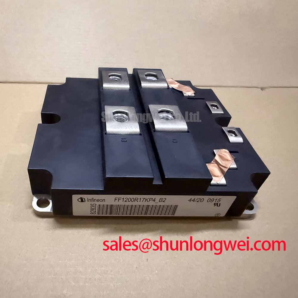
The Infineon FF1200R17KE3_B2 is identified in the supplied factory specification as a 1700.0 V, 1200.0 A IGBT Module in a module package. These are the available official product ratings for this page; switching frequency, gate charge, thermal resistance, junction temperature limit, surge current, isolation voltage, dimensions, and terminal arrangement should be taken from the applicable manufacturer documentation before a retrofit is approved.
| Parameter | Specified value | Classification |
|---|---|---|
| Manufacturer | Infineon | Product identification |
| Part number | FF1200R17KE3_B2 | Product identification |
| Voltage rating | 1700.0 V | Official factory specification |
| Current rating | 1200.0 A | Official factory specification |
| Package | Module | Official factory specification |
Peak junction temperature during a pulsed overload is governed by the complete transient path from semiconductor junction to case, heatsink, cooling medium, and enclosure. A plant maintenance team should therefore review the load waveform rather than judging the module from average current alone. Record pulse duration, repetition rate, DC link conditions, ambient temperature, heatsink temperature, and cooling airflow while the converter is operating under its most demanding duty.
A multi RC thermal model is useful because short overloads are initially controlled by the faster junction to case response, while repeated pulses progressively load slower thermal sections and the heatsink. The engineering calculation should combine the power loss waveform with the applicable transient thermal impedance curve from the manufacturer documentation. The resulting junction temperature estimate must then be checked against the specified peak junction limit and the actual cooling arrangement. A thermal camera reading on the case can support the investigation, but it does not directly measure the silicon junction.
For a wind turbine full scale converter, inspect the thermal path after periods of high reactive power, regenerative operation, or repeated grid support events. Dust on the heatsink, restricted cabinet airflow, degraded thermal compound, uneven mounting pressure, and loose power terminals can all increase the case temperature or create local thermal concentration. The maintenance record should compare temperature rise at equivalent load points rather than relying on one isolated reading.
Mechanical clearance also affects thermal performance. The module base should sit flush against a clean, undamaged heatsink surface, with no burrs, trapped debris, cable interference, or enclosure distortion. The system engineer should determine the mounting method and fastening requirements from the relevant mechanical documentation. Peak electrical margins should be verified during controlled switching tests, especially where the DC link and regenerative braking circuit operate close to the converter design boundary.
FF1200R17KE3_B2 Thermal Electrical Optimization: Active Miller Clamp Implementation Practical Tuning
High dv/dt can transfer current through the off state gate collector capacitance and raise the gate voltage of the opposing IGBT. An active Miller clamp provides a low impedance discharge path during the off state, reducing the chance of unintended turn on. This function belongs to the gate driver implementation, not to the module rating itself, so the driver and module must be evaluated as one switching loop.
Keep the gate drive loop compact, separate the power commutation path from the control return, and place the clamp connection close to the relevant gate and emitter reference. Stray inductance in the emitter return can make the measured gate voltage differ from the driver output. A Kelvin reference may be used only when supported by the module terminal arrangement and the selected driver topology. The engineer should verify the actual terminal definition rather than assuming a universal pin layout.
A negative gate bias may be evaluated as a Design Consideration when the switching environment produces unacceptable Miller-induced gate movement. The permitted bias range, insulation coordination, driver output capability, and turn-on threshold must be taken from the module and driver documentation. It should not be selected from a generic IGBT rule because excessive negative bias can introduce gate oxide stress or interfere with the driver protection scheme.
For a high-side stage, bootstrap sizing begins with a charge budget. The capacitor must supply the gate charge for the commanded switching activity, driver quiescent current, leakage paths, and voltage loss across the charging network while maintaining the required driver supply during the high-side interval. Select the capacitor and charging diode only after the module gate charge, driver consumption, duty cycle, refresh interval, temperature, and switching pattern have been entered into the system calculation. Diode reverse recovery should also be considered because recovery current can disturb the gate supply and add noise to the isolated control circuit.
Industrial drive boards using optocouplers or digital isolators should be checked for common mode transient immunity under the real collector emitter voltage transition. The isolation device, gate driver, clamp circuit, and local decoupling form a signal integrity chain. Infineon’s OptiMOS™ and CoolMOS™ power semiconductor reference material provides broader power switching context, although it is not a substitute for the IGBT module’s own documentation.
Transient Dynamics and Electrical Design: Diagnosing Latent Gate Emitter Dielectric Stress on FF1200R17KE3_B2
Cold bench screening should be performed with the converter isolated, the DC link discharged, and external gate driver connections removed where the circuit permits. Use the digital multimeter diode check function across the main terminals and the antiparallel diode path, recording polarity, displayed forward response, and consistency between equivalent phase positions. A reading that differs materially from a known good assembly deserves further isolation testing rather than an immediate conclusion about the module.
Gate leakage should be checked between each gate and its corresponding emitter reference using an instrument and test method appropriate for the device documentation. Avoid applying uncontrolled insulation tester voltage to the gate terminals. Residual charge from a previous test can distort the result, so allow the gate circuit to discharge through the approved method before repeating measurements. The comparison should include the driver board, gate resistor, clamp device, and connector contamination because an abnormal gate reading may originate outside the module.
When the cold checks are satisfactory, reconnect the driver with current limiting and controlled DC conditions. Observe gate to emitter voltage, collector emitter overshoot, switching-node ringing, and the isolation barrier response with probes that are rated for the circuit. A gate waveform that appears clean at the driver output but is distorted at the module terminals points toward layout inductance, return-path coupling, connector impedance, or probe placement. The next action should be to compare the complete signal path against a known good phase leg.
Moisture and condensation deserve attention in offshore and onshore turbine converter cabinets. Temperature cycling can produce surface contamination around gate connectors and isolation components even when the enclosure appears closed. Maintain the enclosure’s environmental controls, inspect cable glands and ventilation paths, and allow equipment to reach a stable dry condition before energized testing.
Benchtop Waveform Tuning: Mitigating Stress via Drop In Retrofit and Tuning Turn On Turn Off on FF1200R17KE3_B2
When a modern IGBT module is installed on a legacy drive board, the original external gate resistors may not provide the intended switching behavior. Separate turn on and turn off resistance allows the engineer to balance switching loss, voltage overshoot, diode recovery interaction, and di/dt ringing. The initial resistance should be selected as a Typical Starting Point from the driver capability and the module’s documented gate charge, then adjusted only after waveform measurements.
Use a double pulse or equivalent controlled switching test to observe the gate voltage and power loop behavior at the intended DC link condition. Tune turn on behavior while watching collector emitter rise time, reverse recovery interaction, and gate plateau stability. Tune turn off behavior while watching inductive overshoot, negative gate excursion, and the off state margin of the opposing device. The final setting is system determined because busbar inductance, emitter return inductance, driver placement, load current, and snubber configuration all influence the result.
Regenerative braking adds another practical stress path. The chopper and braking resistor must absorb the energy delivered by the mechanical system and DC link without forcing the IGBT beyond its switching or thermal boundary. Confirm the resistor duty profile, chopper timing, DC link protection threshold, and thermal recovery interval during commissioning. For battery backed bidirectional DC to DC systems, repeated charge and discharge cycles can create thermal cycling in the power stage; cabinet cooling, busbar symmetry, and current sharing should be reviewed across the complete cycle rather than at one operating point.
Where a rectifier or front end is part of the same conversion chain, the FZ600R12KE3 may be evaluated as a separate peripheral topology reference. It should not be treated as an automatic replacement or electrically interchangeable device. For a neutral comparison within the same high power module family, engineers may also review FZ1200R17KF6-B2 against voltage, current, mechanical, gate drive, thermal, and protection requirements.
For switching systems that combine IGBT stages, silicon controlled rectifier functions, or auxiliary precharge circuits, gate trigger behavior must be assessed from the actual IGT, VGT, pulse width, and pulse train requirements of the selected thyristor. A strong repeated trigger signal can improve firing consistency, but the gate driver must remain within its current and thermal limits. The same commissioning record should capture precharge timing, braking transitions, isolation response, and the temperature recovery between high energy events.
Long term design reviews may also consult the Wide Bandgap Revolution engineering guide when comparing switching technologies and layout priorities. It provides technology context; it does not change the stated ratings of this Infineon module.
Maintenance Note: Monitor contact temperature and clean the heatsink airflow path at scheduled intervals, while checking thermal interface aging and terminal tightness during each planned shutdown.