

Content last revised on November 7, 2026
Assembly Integrity & Layout Architecture: Preventing Thermal Interface Degradation for FF300R12KS4
Isolate the equipment, verify that the DC link has discharged, and disconnect the gate driver before checking the FF300R12KS4 for terminal damage or abnormal cold-state conduction. Compare equivalent power paths with the circuit disconnected where necessary; a meter reading through connected capacitors, protection components, or driver circuitry cannot establish the condition of the module alone. Record the terminal orientation and existing connections before loosening the power conductors.
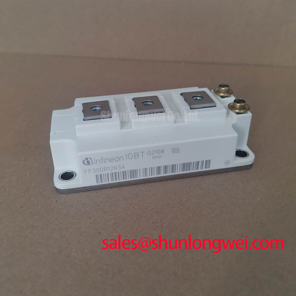
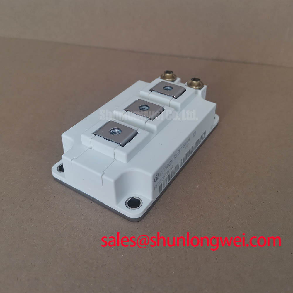
The core specifications for this Infineon device are: Manufacturer: Infineon; Part Number: FF300R12KS4; Collector-Emitter Voltage (Vces): 1200.0 V; Rated Collector Current (Ic): 300.0 A under the datasheet-specified conditions; Configuration / Topology: Dual IGBT module. For replacement assessment, consult the model-specific datasheet for terminal assignments, rating conditions, gate limits, and mechanical requirements. A heavy-duty variable-frequency AC motor drive is one potential integration context, subject to the original equipment’s electrical and mechanical requirements.
Inspect the heatsink contact surface and the removed thermal interface imprint before cleaning away the evidence. Uneven transfer, dry patches, contamination, or material concentrated around the perimeter can help identify contact problems, but none establishes the thermal condition by itself. Compare the imprint with mounting condition, heatsink flatness, cooling performance, and the equipment’s recorded temperature behavior.
As a Design Consideration, control thermal interface material thickness through the approved application process rather than by applying an arbitrary paste depth. The objective is continuous coverage that fills surface irregularities without creating an unnecessarily thick thermal barrier. A stencil, controlled dispensing process, or specified pre-applied interface can support repeatability when approved for the assembly. Check the interface material’s handling instructions and compatibility with the mounting surfaces before selecting the process.
Do not use additional paste to compensate for a visibly distorted heatsink or force the baseplate flat through excessive screw loading. Assess surface condition and permitted flatness against the mounting documentation. Where the assembly accommodates baseplate curvature, follow that defined method rather than introducing improvised shims. Remove particles and hardened residue without gouging the contact face, and keep interface material away from electrical connections.
Field Alert: Use the specified tightening sequence and torque for the module assembly; extra tightening is not a remedy for poor thermal contact.
Progressive, even tightening is an Engineering Recommendation where consistent with the manufacturer’s mounting instructions. Keep mounting fasteners and power-terminal fasteners distinct in the work record because their requirements need not be identical. Support busbars so that alignment errors do not pull against the housing, and preserve the equipment’s required electrical clearances around exposed conductors.
For mechanical compatibility screening, use the FF300R12KS4 mounting drawing rather than assuming compatibility from general module-family information. Likewise, evaluate the FF400R12KT3 only as a separate replacement candidate requiring documented comparison of footprint, terminal arrangement, drive requirements, and switching behavior. A related designation or higher current rating does not establish direct interchangeability.
Assembly Integrity & Layout Architecture: Implementing Dynamic Gate Impedance Control for FF300R12KS4
Trace the gate-drive outgoing and return paths before changing a resistor value. As a Design Consideration, shared inductance between the load-current path and the gate return can alter the voltage actually seen at the device terminals. Keep the gate loop compact and separate from high-current commutation paths, using the designated signal return wherever the documented terminal arrangement provides one. Do not assume a dedicated Kelvin-emitter connection from the housing family alone.
During complementary switching, collector-voltage transitions can couple current into the opposite gate through device capacitance. Assess the driver’s sink capability, return-path impedance, and measured off-state gate excursion together. An active Miller clamp is an Engineering Recommendation for evaluation when the driver architecture supports it; its placement and current path determine whether it can control the local gate voltage effectively. It cannot compensate for a long or poorly routed return connection.
Negative off-state bias is another system-level option, not a prescribed setting for this page. Its suitability depends on the module’s gate limits, driver supply behavior, and transient measurements at the terminals. Check startup, shutdown, and undervoltage behavior as well as steady switching. A driver that produces acceptable waveforms during normal operation still requires assessment while its isolated supply rises or collapses.
Select external gate damping through controlled switching evaluation. Peak source and sink requirements depend on gate charge, the intended transition behavior, and total loop impedance; driver headline current alone does not describe the complete circuit. Adjust turn-on and turn-off paths independently where the existing driver supports that arrangement, observing switching loss, overshoot, and unintended gate movement after each change. Record resistor placement as well as resistance because connection inductance affects the result.
Check the isolation stage against the measured common-mode transient environment. As a Design Consideration, optocoupler or digital-isolator CMTI, isolated-supply coupling, and control-side routing can influence apparent gate-command integrity. Investigate disturbances on both sides of the isolation barrier before attributing every unexpected pulse to the power module. If a system also contains an FF600R12KE3, assess its driver and supply requirements separately; inclusion in a related power topology does not establish shared gate settings or a rectifier function.
Preventing Spurious Faults: Short-Circuit Energy Let-Through Matching Guidelines for FF300R12KS4
Retrieve the original fault sequence before resetting protection or fitting a replacement fuse. Establish whether the recorded event began with a driver fault, an overcurrent indication, a supply disturbance, or a downstream circuit problem. Preserve fault timestamps and examine the protection supply and feedback wiring. A reported short circuit is a starting point for investigation, not proof that the module initiated the event.
As a Design Consideration, distinguish rapid electronic protection from branch fault interruption. Desaturation or other suitable current-sensitive protection can command turn-off during a developing fault, while a semiconductor fuse addresses interruption under its specified circuit conditions. Compare detection delay, blanking, driver response, and controlled shutdown behavior with the model-specific short-circuit limits. Protection timing must be evaluated as a complete chain rather than as the setting of a single device.
Fuse total clearing I²t is relevant to coordination, but it is not automatically an IGBT short-circuit withstand rating. Its applicability depends on prospective fault current, circuit voltage, time-current behavior, and the fuse manufacturer’s stated conditions. Do not infer a permissible module energy limit from the 300.0 A collector-current rating. A fuse comparison alone cannot establish that a failed semiconductor will remain intact or that an enclosure will contain every fault.
For the existing installation, verify the protective device designation, DC interruption suitability, and coordination documentation against the actual DC-link arrangement. Include local capacitor discharge paths in the circuit review: energy stored close to the module may follow a path different from upstream supply current. Inspect busbar supports, cable termination security, and spacing after a fault, since mechanical displacement can change the next energization condition.
Apparent nuisance trips also warrant examination of the sensing circuit. Check the routing and return reference of the fault-detection signal, the integrity of its connectors, and its behavior during normal commutation. Compare the fault signal with simultaneously captured gate and collector-voltage waveforms using appropriately rated instrumentation. If the indication coincides with switching noise, investigate coupling and timing without simply extending blanking or raising thresholds; either change can reduce protection effectiveness and requires system-level validation.
Benchtop Waveform Tuning: Assessing Tail Current and Damping Switching Oscillations on FF300R12KS4
Capture collector-emitter voltage, gate-emitter voltage, and commutation current with a controlled test setup before assigning ringing to diode recovery or IGBT tail current. These phenomena occur during different parts of the switching sequence and should not be treated as interchangeable. Use appropriately rated differential probes and a suitable current sensor, minimize measurement-loop pickup, and check probe timing alignment before comparing peaks.
As a Design Consideration, evaluate the freewheeling diode’s reverse-recovery behavior during commutation under the relevant current and temperature conditions. Peak recovery current and its rate of change affect the stress imposed on the switching path, but neither can be assigned a model-specific value from the voltage and current nameplate ratings. Distinguish actual device behavior from oscillation introduced or exaggerated by probe placement.
Where a sharp recovery transition excites the power loop, examine commutation-path geometry before adding damping components. Minimize unnecessary loop area within the approved assembly and preserve the required insulation spacing. Turn-on gate resistance can be evaluated as a means of moderating commutation, with the resulting switching-energy increase checked against the thermal design. Keep observations from turn-on recovery separate from turn-off tail-current measurements so that a corrective change addresses the relevant event.
An RC snubber is an Engineering Recommendation for assessment when measured ringing justifies it, not a default accessory for the FF300R12KS4. Determine its arrangement and component values from the observed transient, circuit parasitics, and repetitive dissipation. Confirm resistor heating, capacitor pulse capability, and terminal voltage after installation. Component placement matters because a distant snubber can leave the local high-frequency loop insufficiently damped.
For the motor-drive compatibility example, assess reflected-wave behavior at the motor cable separately from module-terminal overshoot. Cable length, termination impedance, and switching-edge behavior influence the remote waveform; a module-side snubber does not automatically protect the motor terminals. Any output filtering should follow measured cable-end behavior and the equipment’s operating requirements.
The Switching loss Application Guide provides related discussion of switching trade-offs, while the Infineon IGBT Modules & Discretes Official Portfolio provides manufacturer product context. After each damping change, repeat the relevant measurements across the intended operating conditions and retain the waveform record with the final driver configuration. Confirm that reduced ringing has not introduced excessive switching loss, slower fault response, or unacceptable component heating.