

Content last revised on October 5, 2026
FP10R12W1T4-B3 IGBT Module Overview
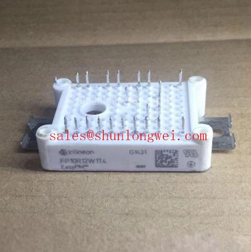
Verify the nameplate, inspect the module housing, and confirm the device rating before connecting the replacement to a live converter or servo drive. The supplied manufacturer data identifies FP10R12W1T4-B3 as an Infineon IGBT Module rated at 1200 V and 10 A. Its listed package category is Module. Pin assignments, switching characteristics, thermal resistance, gate-drive limits, isolation data, and mechanical dimensions should be checked against the original Infineon documentation before installation.
| Parameter | Official supplied specification |
|---|---|
| Manufacturer | Infineon |
| Part number | FP10R12W1T4-B3 |
| Rated voltage | 1200.0 V |
| Rated current | 10.0 A |
| Package | Module |
| Potential evaluation area | High-dynamics multi-axis CNC and robotics servo drives, subject to system verification |
These are the available official product parameters supplied for this product page. They should not be expanded into unverified claims about short-circuit duration, junction temperature, switching frequency, gate voltage, isolation withstand, thermal impedance, lifetime, or certification status. For a complete design review, engineers should consult the applicable Infineon documentation and compare every electrical and mechanical requirement with the installed power stage.
Benchtop Waveform Tuning: Mitigating Stress via Active Miller Clamp Implementation
Begin waveform evaluation with the inverter disconnected from the motor and with the DC link controlled by an isolated laboratory setup. Confirm the gate-driver reference, emitter return, probe connection, and oscilloscope bandwidth before judging the turn-on or turn-off waveform. A poorly referenced probe can display an apparent gate disturbance that is actually a measurement error.
High common-emitter voltage movement during switching can couple through the device Miller capacitance and disturb the inactive gate. An active Miller clamp is a driver-side function rather than an assured feature of the FP10R12W1T4-B3 itself. If the selected driver provides this function, the clamp path should be placed close to the gate and emitter return so that the transient current does not share a long, high-inductance route with the signal reference.
The supplied product information does not specify a negative gate-bias requirement for this module. A negative off-state gate voltage, if considered by the system designer, must be selected from the verified gate-emitter absolute maximum rating, driver capability, isolation arrangement, and switching test results. It should not be treated as a default value for this part. The same principle applies to gate resistance: the final value depends on driver current, gate charge, loop inductance, switching loss, electromagnetic behaviour, and the required dynamic response.
During bench testing, inspect the active and inactive gate signals at the same time as the collector-emitter voltage and phase current. A narrow unintended gate pulse may indicate capacitive coupling, a reference bounce, excessive loop inductance, or driver timing interaction. Verify the signal at the module terminals rather than relying only on a remote driver test point. If the waveform changes substantially after the probe ground arrangement is corrected, repeat the measurement before changing the gate network.
Use the Infineon IGBT Modules and Discretes official portfolio as the manufacturer-level reference for family documentation and application information. The listed 1200 V and 10 A ratings identify the product category and electrical boundary, but they do not by themselves establish the safe operating area for a particular PWM pattern, overload event, or motor-control algorithm.
Pro Tip: Keep the power commutation loop and gate-driver return physically compact, then verify turn-off overshoot and inactive-gate stability with a properly referenced oscilloscope during double-pulse or equivalent switching tests.
Benchtop Waveform Tuning: Mitigating Stress via Common-Mode Transient Immunity
When this module is evaluated in a high-dynamics CNC axis or robotics servo inverter, the gate driver and power module operate across rapidly changing common-mode voltage. The module data supplied here does not state a reinforced isolation withstand value or a common-mode transient immunity rating. Those figures must come from the selected driver, isolation barrier, power supply architecture, and applicable safety documentation. They must not be assigned to the IGBT module without a supporting source.
Review the complete isolation path, including the gate-driver isolator, isolated bias supply, PCB creepage and clearance, connector arrangement, heatsink relationship, and oscilloscope test method. A driver advertised with a high CMTI value may still experience false triggering if the board layout allows displacement current to flow through the control reference or if the isolated supply is poorly decoupled. The result should be evaluated at the module gate and emitter terminals under the highest expected switching stress.
For a high-side driver that uses a bootstrap supply, capacitor selection is a system calculation. The designer should account for the high-side gate charge, driver quiescent current, bootstrap diode or charging path, switching duty cycle, leakage, capacitor bias derating, start-up sequence, and the allowable supply-voltage ripple. The required capacitance cannot be confirmed from the 1200 V and 10 A module ratings alone. Where the servo topology does not provide sufficient refresh time, an isolated high-side supply may require evaluation instead.
Bench troubleshooting should separate power integrity from logic integrity. Monitor the driver supply, input command, gate-emitter voltage, and switching-node voltage on synchronized channels. If an intermittent pulse appears only when the power stage is enabled, compare it with the isolated-supply waveform and common-mode displacement current. If it appears with the power stage disabled, inspect the controller timing and driver enable logic first. This approach avoids assigning a single cause to a complex transient event.
The system integrator should also verify the required supply voltage from the original drive documentation. The supplied product information does not confirm a 3.3 V or 5 V control interface, a specific gate-bias voltage, or a particular driver topology. Interface compatibility is therefore a system-level acceptance item, not an inferred property of the module.
Transient Dynamics and Electrical Design: Evaluating Thermal Capacitance Under Pulsed Load
The 1200 V voltage rating and 10 A current rating are official supplied product parameters, not a complete thermal operating envelope. Actual junction stress depends on conduction loss, switching loss, pulse duration, duty cycle, case temperature, cooling interface, airflow, bus voltage, current waveform, and the electrical characteristics documented for the exact device revision.
For a pulsed overload evaluation, record the case temperature and electrical waveform while applying a controlled load profile. A junction-temperature estimate may use the manufacturer’s transient thermal impedance data and a multi-section RC model when that data is available. The calculation should include the initial thermal condition, the pulse sequence, the cooling interval, and the thermal path from junction to case and from case to heatsink. Without the relevant thermal impedance curves and maximum junction-temperature specification, a numerical peak junction-temperature margin cannot be responsibly stated for this page.
Thermal capacitance is important because a short current pulse does not produce the same temperature response as continuous operation. The die, substrate, baseplate, thermal interface, and heatsink respond over different time scales. Designers should therefore test both isolated pulses and repetitive pulse trains. A waveform that appears acceptable during one pulse may produce a different case-temperature trend when the repetition rate increases.
Use a thermal interface method that is compatible with the verified module mounting instructions, heatsink surface, clamping arrangement, and service environment. The supplied product data does not provide a mounting torque, flatness tolerance, thermal resistance, or interface-material specification. Those details should be taken from the applicable mechanical drawing and assembly guidance rather than borrowed from another module family.
During fault investigation, compare the electrical switching waveform with the thermal measurement and inspect the module mounting area for uneven contact, contamination, loosened hardware, or an unsuitable interface layer. A temperature rise may be associated with excessive switching loss, poor heat transfer, current imbalance, a control-timing issue, or an incorrect measurement location. Confirm the complete chain before replacing the module.
For broader cooling architecture work, the engineering guide The Advanced Thermal Management Revolution provides background on thermal-management approaches. It should be used as a design reference, while the final thermal limits remain governed by the specific Infineon documentation and the measured assembly.
Assembly Integrity and Layout Architecture: Evaluating Long Motor Lead Reflected-Wave Effects
Long motor cables can behave as distributed transmission structures when their electrical length becomes significant relative to the switching edge. Cable impedance, motor impedance, termination behaviour, switching speed, cable shielding, and installation geometry can then influence the voltage seen at the inverter terminals and motor terminals. The supplied module parameters do not specify a permitted motor-cable length, reflected-wave limit, output-filter value, or dv/dt rating.
Evaluate the complete drive installation rather than the IGBT module in isolation. Measure the switching-node voltage at the inverter output and, where practical, at the motor terminals using probes and accessories rated for the measured transient. Compare the result with the verified collector-emitter voltage limit and the system DC-link condition. The design objective is to control overshoot and ringing while maintaining acceptable switching loss; the filter, choke, or cable treatment must be selected from measured system behaviour.
An output filter may reduce motor-terminal stress, but it can also alter current control, resonance behaviour, leakage current, acoustic noise, and semiconductor switching loss. Any dv/dt filter or common-mode choke should therefore be validated with the actual motor, cable, carrier settings, grounding arrangement, and protective devices. Do not assume that a filter value used on another inverter is suitable for this module or this servo axis.
Keep the DC-link connection, commutation path, and phase output layout symmetrical where the mechanical design permits. Separate control wiring from high-current switching conductors, provide a defined shield termination strategy, and verify that the heatsink and enclosure do not create an unintended return path for common-mode current. These are design considerations, not official specifications of FP10R12W1T4-B3.
For service replacement, compare the original module’s terminal arrangement, mounting pattern, electrical rating, thermal path, and driver compatibility before considering another device. The FP10R12KE3 can be reviewed as a separate compatible-device candidate during material planning, but substitution requires a documented electrical, mechanical, thermal, and control-interface comparison rather than a rating-only decision.
⚠️ Field Alert: Isolate and discharge the DC link before disconnecting the module or motor cable, then verify the absence of hazardous voltage with an appropriately rated instrument.