Content last revised on September 10, 2026
Thermal Time Constants (tau_i) and Peak Junction Temperature Margin Calculation
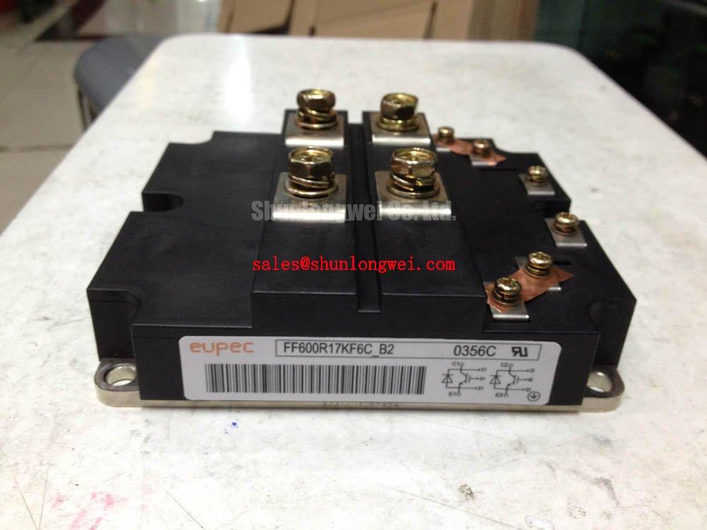
Incoming quality verification of high-power switching modules demands rigorous thermal modeling alongside static bench screening. The FF600R16KF4 dual IGBT module from Infineon is rated for a continuous collector current of 600A (Official Datasheet Specification) with a collector-emitter breakdown voltage of 1600V (Official Datasheet Specification). In demanding heavy rail traction converters and locomotive propulsion drives, the module encounters cyclic acceleration profiles that inject severe transient thermal pulses into the silicon dice. Evaluating these cycles requires calculating the transient thermal impedance across multiple RC time constants rather than relying solely on the steady-state thermal resistance junction-to-case of 0.024 K/W (Official Datasheet Specification).
During heavy freight locomotive starts, high collector current pulses induce transient heat flux through the silicon die, the solder interface, the direct copper bonded (DCB) ceramic substrate, and the copper baseplate. When calculating peak junction temperature (Tvj) margins against the absolute maximum rating of 150°C (Official Datasheet Specification), engineers apply a 4-layer Foster thermal network. The shortest thermal time constants (τ1 ≈ 0.001 to 0.01 s) dictate the immediate temperature rise of the IGBT junction during sub-second stall torque demands. Intermediate constants (τ2, τ3 ≈ 0.05 to 0.5 s) reflect heat spreading across the ceramic isolation barrier, while the longest constant (τ4 > 1 s) represents baseplate thermal saturation into the liquid-cooled heatsink.
💡 Bench Tip: During incoming quality inspection on the bench, static cold-state forward voltage measurements provide an immediate indicator of internal die bonding integrity. When checking with a calibrated 4-wire Kelvin sensing setup at a low test current (such as 10A at 25°C ambient), verify that the antiparallel freewheeling diode drop and the active IGBT forward conduction remain within nominal manufacturing variance. Any abnormal shift in cold-state drop often points to packaging stress or internal interconnect non-uniformity.
Achieving calculated junction margins in physical assemblies relies directly on proper thermal interface material (TIM) deposition and mechanical fastening. A non-uniform TIM layer creates localized hot spots that invalidate Foster network models. Apply a screen-printed or roller-applied silicone-free thermal grease at a controlled thickness between 50 μm and 100 μm across the baseplate. Fasten the module baseplate to the machined cold plate using an initial cross-pattern pre-tightening, followed by final torque calibration to 4.25 Nm (Official Datasheet Specification). For the high-current power terminals, tighten the M8 bolts to exactly 10 Nm (Official Datasheet Specification) using calibrated torque wrenches to prevent internal lead-frame shearing or contact resistance thermal runaway under vibration.
Static and Dynamic Current Distribution across Paralleled IGBT Switches
High-power traction propulsion platforms often require paralleling multiple half-bridge switches to handle megawatt-scale envelope requirements. The FF600R16KF4 exhibits a typical on-state saturation voltage VCE(sat) of 2.30V (Official Datasheet Specification). At operating temperatures approaching 125°C to 150°C, the silicon exhibits a positive temperature coefficient of saturation voltage. This physical characteristic provides inherent negative feedback for static current sharing: as one paralleled module draws higher current, its junction temperature rises, increasing its internal VCE(sat) and naturally shunting excess current to cooler adjacent devices.
Dynamic current sharing during sub-microsecond turn-on and turn-off transients is dominated by loop parasitic inductance and gate driver symmetry rather than semiconductor channel characteristics. Stray busbar inductance must be strictly contained, with a recommended target of less than or equal to 25 nH across the DC link connection. Under heavy di/dt switching transitions, parasitic inductance induces severe overvoltage spikes across the main terminals. Mitigating these spikes requires placing low-inductance polypropylene snubber film capacitors directly across the module DC input terminals, combined with laminated copper busbar sandwich structures that maximize mutual inductance cancellation.
For auxiliary traction sub-systems requiring lower current handling, engineers frequently evaluate scaled counterparts such as the FF150R12ME3G, which operates within a 1200V architecture. In higher voltage central DC traction links, engineers often interface these stages alongside primary power devices like the FZ1000R33HE3 to balance multi-level inverter voltage distribution.
⚠️ Field Alert: Asymmetrical gate routing across paralleled modules creates dynamic current imbalance during hard switching. Keep gate-emitter trace lengths identical, use twisted-pair or shielded coaxial drive lines, and provide individual gate resistors (RG,on and RG,off) directly at each module terminal rather than driving parallel gates from a single shared resistor.
Long Motor Lead Reflected Wave Voltage & Motor Terminal Insulation Protection
In locomotive bogie configurations, inverter cabinets are separated from traction motors by long shielded cable runs spanning 10 to 30 meters. The rapid switching transitions of the FF600R16KF4 generate high voltage slew rates (dv/dt) that interact with cable transmission line characteristics. When the characteristic impedance of the traction cable (typically 50 to 100 Ω) mismatches the high impedance of the motor stator winding, transmission line reflection causes voltage doubling at the motor terminals. With DC bus operating voltages of 900V to 1100V, reflected wave peaks can exceed 2000V, degrading stator winding turn-to-turn insulation and accelerating partial discharge breakdown.
Controlling terminal overvoltage requires dedicated dv/dt filters, sinusoidal output filters, or series motor chokes placed at the inverter output. Sizing these magnetic components balances filter losses against insulation stress mitigation, typically targeting motor terminal dv/dt rates below 500 V/μs. In addition, gate resistor selection directly regulates internal IGBT turn-on and turn-off speeds. Tuning RG,off upward dampens terminal dv/dt at the cost of incremental switching loss, creating a thermal-insulation trade-off that bench testing engineers must quantify.
Comprehensive failure analysis procedures for power switching assemblies exposed to long cable reflections are documented in the Field Engineer’s Handbook. For detailed architectural data on high-power planar and trench-gate switching structures, consult the Infineon IGBT Modules & Discretes Official Portfolio.
Dead-time management in the gate drive firmware protects against bridge leg shoot-through during cross-conduction intervals. For the FF600R16KF4, maintain a minimum hardware-enforced dead-time between high-side and low-side switching commands (Design Consideration: 3.0 μs to 5.0 μs typical for 1600V modules) to allow complete collector current decay and diode reverse recovery clearance before the opposing switch initiates turn-on.
Common-Mode Transient Immunity (CMTI > 100kV/us) in Harsh Industrial Environments
The switching of 600A collector currents across 1600V potential barriers generates intense electromagnetic fields within the converter enclosure. High dv/dt transitions couple common-mode displacement currents across gate drive isolation barriers, power supply transformers, and control ground planes. To prevent catastrophic shoot-through events caused by false gate triggering, the isolation barrier between primary control logic and secondary gate drive stages must support high common-mode transient immunity, with target ratings of CMTI > 100 kV/μs.
The FF600R16KF4 incorporates an internal electrical isolation test voltage rated at 4.0 kV RMS (Official Datasheet Specification) for 1 minute between the baseplate and power terminals. Maintaining system-level isolation integrity requires maintaining layout clearance and creepage distances that comply with industrial rail standards. Secondary gate drive power supplies must utilize low-coupling-capacitance DC-DC converters (barrier capacitance ≤ 3 pF) to restrict common-mode current flow back into the digital signal processor (DSP) domain.
| Parameter | Specification Value | Engineering & Testing Implication |
|---|---|---|
| Collector-Emitter Breakdown (VCES) | 1600V | Provides operational safety margin for 900V–1100V DC rail catenary buses. |
| Continuous Collector Current (IC) | 600A | Continuous rating requiring low-inductance busbars and calibrated cooling. |
| Saturation Voltage (VCE(sat)) | 2.30V (Typical) | Positive temperature coefficient enables steady-state parallel current sharing. |
| Isolation Test Voltage (Visol) | 4.0 kV RMS (1 min) | Galvanic baseplate isolation supporting high safety margins. |
| Thermal Resistance (Rth(j-c)) | 0.024 K/W | Thermal path requiring 50–100 μm uniform TIM layer for peak heat flux. |
| Baseplate Mounting Torque | 4.25 Nm | Critical mechanical fastening torque to prevent baseplate bowing. |
| Terminal Fastening Torque | 10 Nm | M8 power terminal tightening torque to minimize contact resistance. |
Implementing an Active Miller Clamp on the low-side and high-side gate drive circuits eliminates parasitic turn-on induced by high dv/dt collector-emitter transitions. When the gate voltage drops below approximately 2.0V during commanded turn-off, the Miller clamp engages an ultra-low impedance path directly to the emitter rail, shunting dynamic gate displacement currents and stabilizing the gate below the gate-emitter threshold voltage VGE(th).