

Content last revised on September 21, 2026
FF600R17KF6C_B2 Circuit Protection & Reliability: Turn-Off Vpeak Control
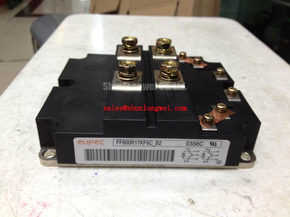
In a high-power converter repair, the first electrical concern is whether the original DC bus, laminated busbar, snubber network, and gate-drive timing remain suitable for the installed FF600R17KF6C_B2. The module’s 1700V official voltage rating identifies its device class, but it does not replace measurement of actual switching stress in the finished equipment.
At IGBT turn-off, the voltage seen by the switch is influenced by DC-link voltage and stray inductance in the commutation loop. In engineering terms, the observed peak follows the relationship Vpeak equals VDC plus stray inductance multiplied by the rate of current change. This is an Engineering Calculation principle, not an official switching-overvoltage guarantee for this module. The final peak depends on the inverter geometry, busbar path, capacitor placement, gate drive, load current, measurement probe arrangement, and transient behavior of the complete circuit.
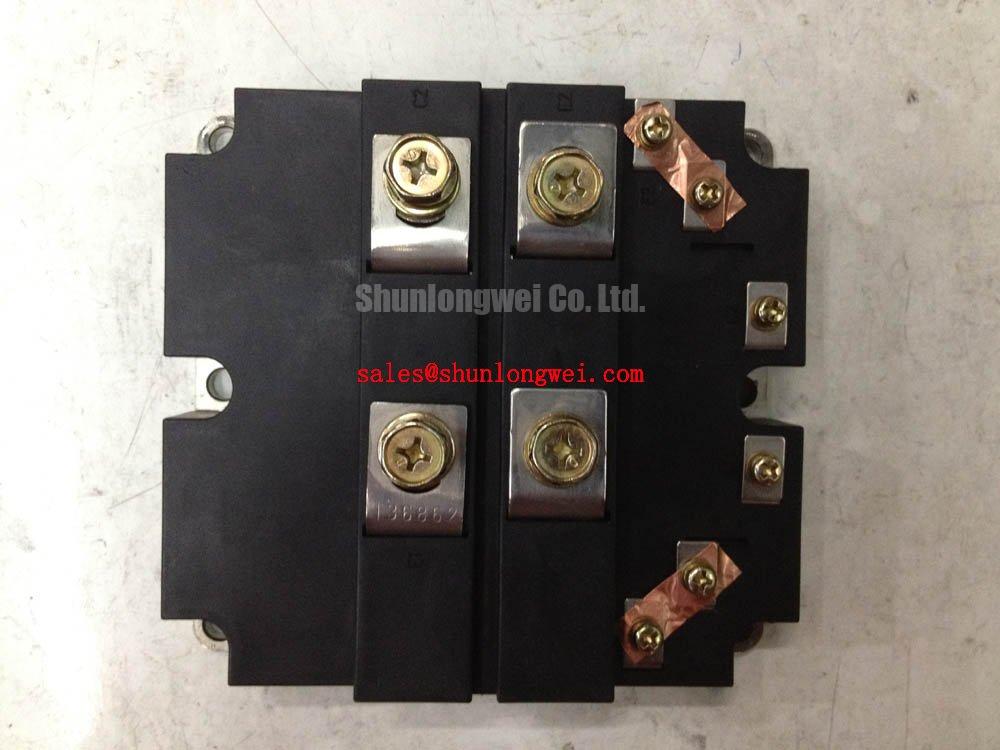
A practical inspection begins with the physical current loop. Check whether the DC-link capacitor connections remain close to the power terminals, whether positive and negative conductor paths are routed with low enclosed area, and whether the mechanical busbar stack has remained flat and aligned after servicing. Uneven terminal interfaces, added cable length, loose hardware, or altered busbar routing can increase loop inductance and make turn-off overshoot more severe.
Where a snubber circuit is present, it should be treated as part of the original converter design rather than a generic accessory. Its capacitor, resistor, conductor placement, and thermal condition should be checked against the equipment schematic. A degraded snubber may contribute to ringing or repetitive stress, but waveform evidence is needed before assigning it as the sole fault mechanism. Measure voltage at the module connection using an appropriate differential measurement method and compare the result with a known-good phase leg or validated commissioning record where available.
⚠️ Field Alert: Isolate and discharge the DC-link energy storage system according to the equipment safety procedure before removing gate-drive or power connections.
Design Consideration: A symmetrical planar busbar arrangement can help reduce commutation-loop inductance and support more balanced current paths during switching. The system engineer should validate the resulting turn-off peak margin with double-pulse or equivalent switching tests under representative DC-link voltage, load current, temperature, and gate-drive conditions.
For a utility-scale 1500V central solar photovoltaic inverter, this evaluation is especially relevant because the installed DC bus can operate near the voltage class of the switching devices. The 1700V rating should be assessed together with measured transient excursions rather than being treated as a standalone system-voltage approval.
Field Diagnostics & Commissioning: Reliability Assessment in FF600R17KF6C_B2 Topologies
Commissioning should begin with objective checks that separate module condition from surrounding-system faults. With the converter safely isolated, technicians can inspect terminal torque condition, cooling interface continuity, gate-driver connector seating, DC-link capacitor condition, and evidence of localized overheating on busbars or driver boards. Cold resistance checks can identify obvious unintended low-resistance paths, but they cannot establish switching integrity, dynamic current sharing, or short-circuit protection performance.
Desaturation protection belongs to the gate-drive system, not to the published identity parameters of the FF600R17KF6C_B2. The driver monitors collector-emitter behavior during commanded conduction and reacts if a fault condition is detected. Its response timing, blanking arrangement, soft turn-off sequence, and fault latch behavior must be verified from the original gate-driver documentation. Do not assume that a particular detection time or turn-off profile is inherent to this IGBT module unless it is explicitly stated by the original equipment manufacturer.
A two-stage controlled turn-off strategy is commonly considered in high-energy converter systems because an abrupt interruption of fault current can create excessive inductive voltage stress. This is a Design Consideration. The correct protection sequence must be established from the driver design, measured switching waveforms, module limits documented for the exact assembly, and the protection philosophy of the inverter.
Altitude, terrestrial neutron exposure, single-event burnout behavior, and failures-in-time calculations require source-specific device data and a defined mission profile. No quantitative FIT rate, altitude derating value, or single-event burnout probability is stated here for the FF600R17KF6C_B2. Engineers evaluating installations at elevated sites should obtain the applicable system-level reliability documentation and assess DC-bus operating conditions, semiconductor derating policy, environmental exposure, and protection response through controlled verification.
When a repaired inverter shows recurring phase-leg trips, avoid treating a single symptom as proof of a single root cause. Compare gate command signals, collector-emitter voltage waveforms, current sensor outputs, protection-latch records, and DC-link ripple against an unaffected phase or a validated reference unit. The Field Engineer’s Handbook provides a useful reference path for organizing power-semiconductor test observations and fault-analysis records.
For replacement evaluation, a module such as FF45017ME4 may appear in sourcing discussions within the same broad voltage class, but it should not be presumed interchangeable. Current capability, mechanical arrangement, gate-drive compatibility, thermal behavior, protection settings, and original inverter documentation must all be reviewed before any substitution decision.
Benchtop Waveform Tuning: Gate Drive Isolation and False-Trigger Prevention
Before energizing a repaired power stage, confirm that every gate-drive channel is referenced correctly to its intended emitter or return node and that no connector pin, optical interface, isolation barrier, or auxiliary supply path has been disturbed. The IGBT module itself is a power switching element; reinforced isolation rating and common-mode transient immunity are characteristics that must be verified for the specific gate-driver and isolation components used by the equipment.
False turn-on can occur when rapid collector voltage movement couples through the power circuit and gate network. This can be aggravated by long gate leads, poorly controlled return routing, mismatched driver channels, inadequate emitter reference routing, or altered busbar geometry. A bench investigation should therefore examine gate-emitter voltage at the module connection while observing the corresponding collector-emitter switching waveform. Measurements should be made with instrumentation suitable for the circuit voltage and transient environment.
Engineering Recommendation: Keep the gate-drive loop compact, pair each gate connection with its intended return path, and preserve the original driver-board layout wherever practical. These measures aim to reduce susceptibility to induced gate disturbance during high-voltage transitions. The acceptable waveform behavior must be determined by the complete inverter design and verified during controlled switching tests.
Dead-time coordination should also be confirmed at the control level. Dead time is necessary to prevent unintended simultaneous conduction in a switching leg, yet excessive dead time can alter waveform quality and loss distribution. There is no universal value that can be assigned from the official 1700V and 600A identification ratings alone. Designers should use the original controller documentation and test records to validate timing across temperature, load, and DC-link operating conditions.
Where an isolated driver supply includes bootstrap or charge-pump circuitry, check the original driver schematic for diode orientation, capacitor condition, and voltage behavior during the intended switching sequence. These supporting circuits are system-specific. Their correct operation should be demonstrated through supply-rail and gate-command measurements rather than inferred from module package type.
Transient Dynamics & Electrical Design: Junction-to-Case Thermal Network Evaluation
The thermal condition of an FF600R17KF6C_B2 installation depends on conduction loss, switching loss, pulse duty, heatsink performance, coolant or airflow condition, mounting pressure, interface material, and the temperature of adjacent components. The official parameters provided identify the module as a 1700.0V, 600.0A Infineon IGBT module; they do not by themselves provide a complete thermal model for a particular inverter assembly.
For pulsed overload analysis, system engineers commonly use the manufacturer’s transient thermal impedance information and a multi-section thermal network to estimate the relationship between dissipated energy and junction response over time. This is an Engineering Calculation process that requires the exact datasheet thermal curves, switching-loss data, heatsink boundary conditions, and measured load profile. Without those inputs, assigning a junction-temperature margin or overload duration would be speculative.
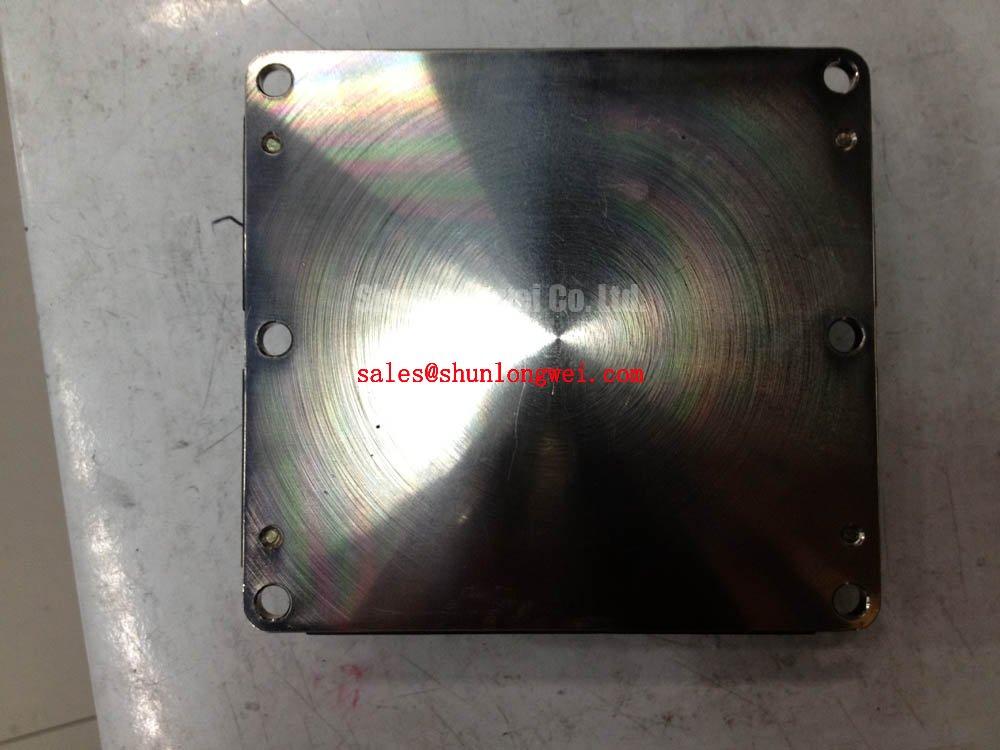
During service work, inspect the heatsink contact surface for flatness, contamination, corrosion, and remnants of degraded interface material. Verify that mounting hardware is tightened according to the original equipment assembly requirement and in the correct sequence. Uneven clamping can produce localized thermal resistance variation, while an altered cooling path can make a healthy module appear electrically unstable under load.
Thermal diagnosis is more reliable when it combines several observations: heatsink temperature trend, cooling-system flow or fan status, phase-current balance, switching waveform quality, protection-event history, and repeated-load behavior. A rising temperature trend may indicate a cooling-path concern, higher loss, a control imbalance, or another system condition. It should be investigated with measured evidence rather than attributed automatically to the module.
For central solar inverter integration, engineers should verify that the installed cooling assembly, DC-link arrangement, gate-drive protection scheme, and power-module mounting pattern remain consistent with the original inverter design. This approach keeps the FF600R17KF6C_B2 within an evidence-based electrical and thermal evaluation process while respecting the operating limits established by the equipment manufacturer.

