
Content last revised on November 3, 2026
Assembly Integrity & Layout Architecture: Managing Long Motor Lead Reflected Wave Voltage for FP50R12KS4C
- Check for unintended short circuits and verify the insulation condition using the manufacturer's permitted test method before applying the DC link.
- Inspect the baseplate, thermal interface, heatsink contact, and clamping arrangement for even mechanical support.
- Confirm the gate driver reference, turn off behavior, desaturation protection path, and gate loop return connection.
- Compare the installed motor cable arrangement with the drive output filter and switching test configuration.
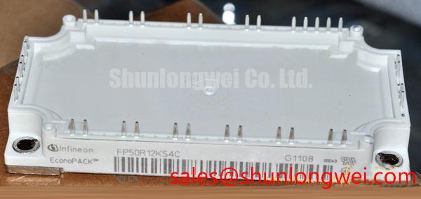
The Infineon FP50R12KS4C is a 1200 V, 50 A IGBT module with a specified maximum junction temperature of 150°C. Its listed electrical characteristics include a typical VCE(sat) of 1.95 V at IC = 50 A, VGE = 15 V, and Tvj = 25°C. The continuous DC collector current is specified at 50 A with TC = 80°C. These values form the starting point for evaluating the module in a heavy duty variable frequency AC motor drive, subject to the complete switching, thermal, busbar, and protection conditions of the equipment.
| Parameter | Value | Specification context |
|---|---|---|
| Collector emitter voltage, VCES | 1200 V | IGBT blocking voltage rating |
| Continuous DC collector current, IC | 50 A | Specified at TC = 80°C |
| Collector emitter saturation voltage, VCE(sat) | 1.95 V typical | At IC = 50 A, VGE = 15 V, Tvj = 25°C |
| Rectifier diode repetitive peak reverse voltage, VRRM | 1600 V | Input rectifier rating; not the inverter freewheeling diode rating |
| Rectifier diode forward voltage, VF | 1.05 V typical | At IF = 50 A and Tvj = 150°C |
| NTC rated resistance, R25 | 5 kΩ | Temperature monitoring element rating |
| Maximum junction temperature, Tvj max | 150°C | Maximum specified junction temperature |
Long motor leads can turn a normal inverter switching edge into a reflected wave problem at the motor terminals. The cable and motor do not present a simple lumped load at every switching instant. Their characteristic impedance, termination behavior, cable length, and output filter arrangement can produce terminal voltage overshoot that is substantially higher than the drive DC link voltage. A commonly discussed upper condition is a terminal spike approaching twice the applied DC voltage, but the actual waveform must be measured on the installed system rather than assumed from cable length alone.
For the FP50R12KS4C, the first design task is to control the commutation loop formed by the DC link capacitors, power interconnections, module terminals, and return path. Minimize the physical area of the high current switching loop and keep the forward and return conductors closely coupled. Closely coupled PCB power planes or a suitable laminated busbar arrangement can reduce parasitic inductance, while uncontrolled wiring between the capacitor bank and module can increase turn off overshoot. The resulting voltage must be checked against the module voltage rating and the complete protection strategy during representative switching tests.
Output chokes and dv/dt filters should be selected from the motor cable impedance, motor insulation requirements, carrier frequency, common mode behavior, and measured terminal waveform. The correct filter is therefore a system decision rather than a fixed accessory specification of the module. When commissioning a heavy duty variable frequency AC motor drive, measure both the inverter output terminals and the motor terminals with a properly rated differential probe. Check positive and negative switching events, phase to phase voltage, and phase to earth voltage. A waveform that appears acceptable at the inverter can still produce a more severe condition at the remote motor.
Clearance and creepage around the DC link and switching terminals should remain consistent with the working voltage, pollution environment, insulation system, and applicable equipment standard. Avoid routing gate control wiring beside high current motor output conductors. The gate return should follow the intended driver reference path, and control cables should be secured so vibration cannot alter their position against power conductors. The FP50R12KS4C voltage rating is 1200 V; it does not by itself certify the complete drive insulation system or its EMC performance.
When comparing a replacement option, compare topology, voltage rating, current definition, thermal reference point, terminal arrangement, driver behavior, and mechanical envelope together. The FZ2400R12HE4_B9 can be reviewed as a separate high power IGBT module reference, but substitution requires electrical and mechanical validation rather than a rating-only comparison.
FP50R12KS4C Operational Boundaries: Evaluating Dynamic Gate Impedance Control for Robust Limits
High dv/dt at one switch can couple through the Miller capacitance of the opposite switch and create unintended gate movement. In a half bridge, this can reduce the effective dead time and increase the possibility of cross conduction. The FP50R12KS4C should therefore be evaluated with the actual gate driver, gate resistor arrangement, isolated supply, gate return geometry, and power loop used in the drive.
An active Miller clamp can provide a low impedance turn off path after the gate voltage falls below its clamp threshold. A negative gate bias may also be evaluated where the driver and module documentation permit it. The final gate voltage, clamp threshold, switching speed, and turn off condition must be established from the applicable driver and module documentation, then verified with a suitably rated differential or isolated probe at the module gate terminals.
Desaturation protection should be coordinated with the module switching behavior. A hard short circuit, an overcurrent event, and a slow motor acceleration overload do not create identical VCE waveforms. A controlled soft turn off can reduce the rate at which current falls through the commutation loop, but its timing and gate profile are determined by the driver implementation. The protection circuit should be tested with the complete DC link, load inductance, gate loop, and fault detection path installed.
The thermal interface is part of the electrical operating boundary because junction temperature changes affect conduction loss, switching behavior, and available thermal margin. Apply the selected TIM uniformly across the baseplate and prevent voids, contamination, or excessive material from reducing contact quality. The correct thickness depends on the module installation guidance, surface finish, flatness, interface material, and assembly process.
Use the manufacturer's tightening sequence for the heatsink fasteners so the baseplate is supported progressively. The required torque is determined by the module mechanical documentation, fastener specification, washer arrangement, heatsink design, and clamping method. Record the assembly sequence and inspect the thermal interface after a first installation trial. A reliable electrical test can still be invalid if the baseplate is locally lifted or the pressure distribution is uneven.
Bench diagnostic: do not connect or disconnect the gate cable while the DC link or isolated driver supply remains energized.
Transient Dynamics & Electrical Design: Power Connection Integrity on FP50R12KS4C
Power connection assembly must transfer current without placing mechanical stress on the module terminals or internal conductor joints. Misaligned circuit boards, forced terminal alignment, or unsupported power conductors can apply stress to the connection area before the drive is energized. During vibration and thermal cycling, that stress can damage connections and create intermittent heating.
Start with the terminal geometry and connection process specified for the module and the mating circuit board. The board should align with the terminals without forcing them sideways or using the module mounting fasteners to pull the assembly into position. Follow the applicable assembly documentation for terminal insertion, soldering, and mechanical support.
Inspect the installed connections for alignment and solder joint quality. A defective connection can show acceptable continuity at low current while developing a localized temperature rise during drive operation. Measure voltage drop across the connection under a controlled load and compare the thermal image of matching phase connections. Temperature differences are a prompt for further inspection, not proof of a single failure mechanism.
The DC link and output conductors should be supported independently from the module terminals. This prevents cabinet vibration, cable weight, and thermal expansion from being transferred directly into the connections. Flexible motor connections can be useful where movement is expected, but their bend radius, strain relief, insulation clearance, and electromagnetic arrangement remain system design matters.
For a replacement installation, record terminal polarity, phase order, mounting-hole alignment, and driver connections before removing the existing module. Confirm that the replacement’s physical interface matches the circuit board and heatsink. An electrically compatible module can still be unsuitable when its terminal positions force longer commutation paths or alter the gate loop routing.
FP50R12KS4C Thermal-Electrical Optimization: Thermal Time Constants and Peak Junction Practical Tuning
Peak junction temperature during a pulsed overload depends on the complete loss profile and the thermal impedance path from semiconductor junction to case, interface, heatsink, and cooling system. The listed 150°C maximum junction temperature is an upper boundary, not a target operating point. Use the specified 1.95 V typical VCE(sat) condition as a reference point only, because conduction loss changes with current, gate voltage, junction temperature, and switching state.
A practical thermal model can represent the junction to case path with several RC sections so that short pulses and longer overloads are treated differently. For each switching interval, determine the conduction and switching energy from measured or documented device behavior, then apply the relevant transient thermal impedance. The resulting junction temperature rise should be added to the case temperature measured at the manufacturer's specified reference location. A single steady state thermal resistance is not sufficient for every overload waveform.
The 50 A continuous DC collector current specification is stated at TC = 80°C. It should not be interpreted as an unrestricted current value for every PWM duty cycle, switching frequency, ambient condition, or heatsink arrangement. Designers should evaluate RMS phase current, peak current, modulation index, overload duration, cooling airflow, and the temperature contribution of the inverter freewheeling diodes. The listed 1.05 V typical forward voltage at IF = 50 A and Tvj = 150°C applies to the input rectifier diodes; inverter freewheeling diode losses require their own specified characteristics.
The integrated 5 kΩ NTC rated resistance at 25°C can support temperature supervision when the control system uses a characterized sensing circuit. Connect the sensing network according to the control cabinet design and establish alarm behavior from the measured thermal response. The NTC reading should be interpreted with sensor wiring resistance, ADC resolution, filtering, placement, and thermal lag in mind. It is a monitoring input, not a replacement for correct heatsink design or junction-temperature analysis.
Case temperature should be measured at a repeatable location and under a defined load sequence. Log the DC link voltage, phase current, switching frequency, ambient condition, heatsink temperature, and NTC response together. If the measured case temperature rises while the NTC response remains nearly unchanged, inspect sensor coupling and wiring before assigning a semiconductor fault. Thermal transients can also expose mounting pressure variation or TIM distribution problems that are not visible during a short electrical test.
Material selection and assembly quality affect the long-term thermal path. Infineon’s information on .XT Technology provides useful industry context for power module interconnection and thermal reliability discussions, while Infineon OptiMOS™ Low Voltage MOSFETs describes a different semiconductor product family and should not be treated as a specification source for this IGBT module.
For switching technology comparisons, the article The 1200 V CoolSiC™ MOSFET Advantage in Three-Phase Power Conversion can provide background on a different 1200 V device platform. Its discussion does not change the FP50R12KS4C ratings or establish a direct replacement relationship. Any alternative technology must be evaluated against the drive’s gate control, short circuit behavior, thermal model, protection timing, and mechanical interface.