



Content last revised on October 5, 2026
FS75R12KS4 Thermal Electrical Optimization for High C Rate Battery Cycling
| Parameter | Official Specification |
|---|---|
| Manufacturer | Infineon |
| Part Number | FS75R12KS4 |
| Product Category | IGBT Module |
| Package | Module |
| Rated Voltage | 1200 V |
| Rated Current | 75 A |
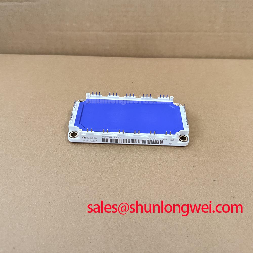
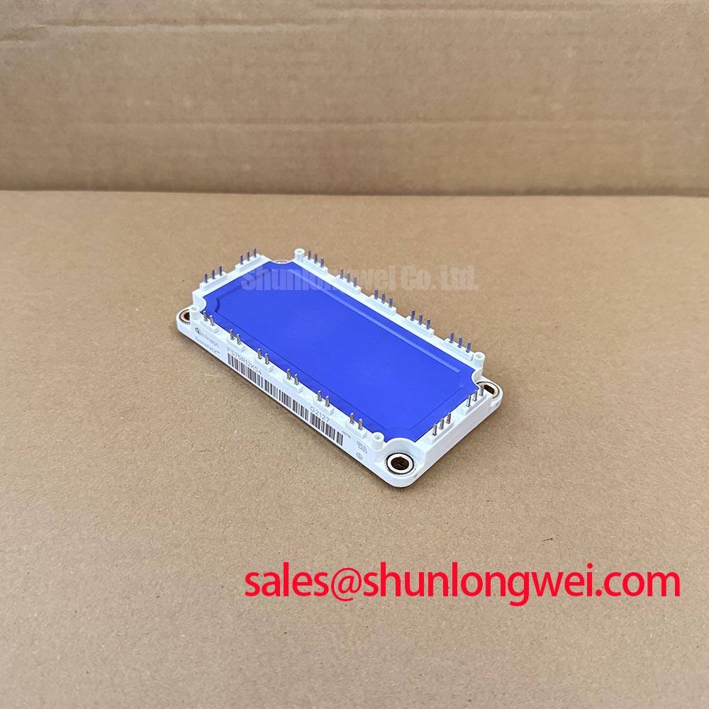
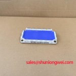
Measure the temperature rise at the module baseplate, DC terminals, and inverter output connections while the battery system moves through charge, discharge, and peak shaving transitions; compare each reading with a known stable operating condition before changing gate drive or cooling parameters. The FS75R12KS4 is an Infineon 1200 V, 75 A IGBT Module in a module package, so the usable operating point in a commercial string inverter or micro grid energy storage system depends on switching frequency, current waveform, cooling path, modulation strategy, and the surrounding protection network rather than on the nameplate current alone.
Four quadrant active power flow places different thermal demands on the inverter bridge. During battery charging, the current direction and switching pattern can produce a different loss distribution from battery discharge or regenerative operation. Peak shaving adds repeated transitions between these conditions. For commissioning, record collector emitter voltage behavior, gate emitter waveform quality, phase current, heat sink temperature, and the timing of thermal rise during both directions of power flow. A temperature increase that appears only during one quadrant may point toward unequal switching loss, busbar asymmetry, gate timing variation, or an external connection problem rather than a simple continuous current overload.
Use a short, mechanically stable DC link connection between the energy storage interface and the inverter bridge. The positive and negative conductors should follow a controlled, symmetrical route so that the commutation loop does not acquire unnecessary stray inductance. This is a Design Consideration, not an FS75R12KS4 factory limit. The system engineer should verify the resulting voltage overshoot with a differential probe during the highest expected current transition and compare the measured peak with the complete DC link protection boundary.
Regen braking choppers and large braking resistors require separate attention when an inverter can receive energy faster than the battery or grid interface can absorb it. Check the chopper command, resistor connection, thermal sensor, and fault feedback as one protection chain. A healthy IGBT module cannot compensate for a braking resistor with degraded connections, a cooling restriction, or a control signal that remains active after a fault. The semiconductor fast fuse should be coordinated with the complete short circuit protection strategy, including the fuse I²t characteristic, wiring impedance, prospective fault current, and the module’s specified short circuit capability where documented. Do not infer a safe fuse match from the 75 A rating alone.
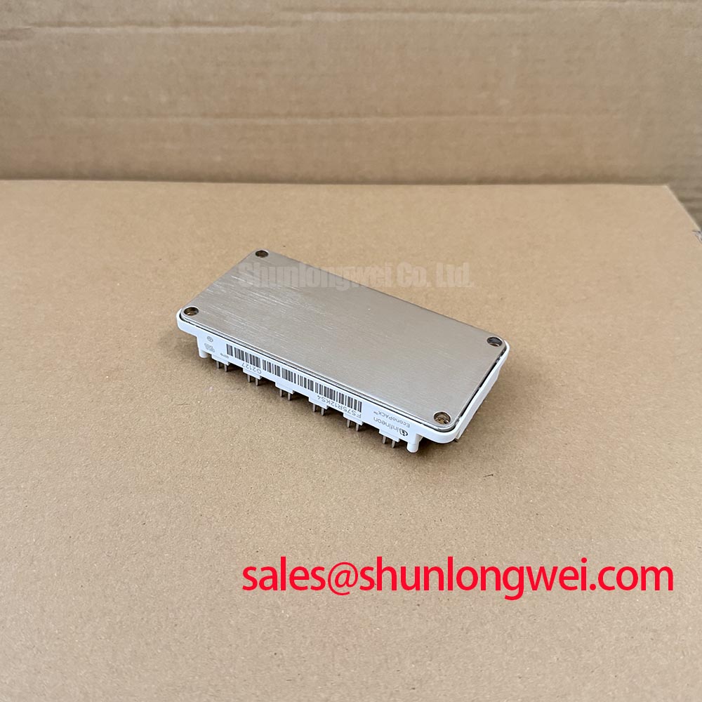
Baseplate preparation has a direct effect on thermal impedance. Remove old thermal interface material, inspect the mating surfaces for burrs or contamination, and apply a uniform, controlled layer suitable for the selected heat sink and mounting method. The correct compound quantity and mounting torque are system and hardware dependent; use the module manufacturer’s mechanical documentation and the heat sink supplier’s instructions rather than treating a general workshop value as an official parameter. Tighten progressively in the specified sequence so that the baseplate remains evenly seated.
In a preventive maintenance program, trend contact temperature at comparable load points instead of relying only on an occasional visual inspection. Clean dust from the heat sink and fan path, inspect for blocked filters, and check whether moisture or condensation has affected the enclosure. ⚠️ Maintenance Note: Monitor contact temperature and verify the cooling airflow after cleaning, because a clean heat sink cannot correct a loose power terminal or deteriorated thermal interface.
For a neutral cross reference during service planning, engineers may evaluate FS100R12N2T4 as a separate device option, but its electrical, mechanical, gate drive, and protection requirements must be compared independently. A higher current number does not by itself establish interchangeability.
Preventing Spurious Faults with Symmetrical Busbar Geometry
Probe the DC bus directly at the module power terminals and compare the positive and negative commutation paths when a false overcurrent or gate fault occurs. Look for unequal probe loop placement, ringing that appears on only one bridge leg, and voltage disturbance coupled into the gate driver reference. Symmetrical busbar geometry helps reduce differences between parallel current paths, but the final result must be validated on the assembled inverter rather than assumed from a drawing.
When several IGBT paths operate in parallel, static current sharing and dynamic current sharing are separate checks. A positive temperature coefficient of forward voltage in the relevant operating region can support static current balancing in parallel semiconductor arrangements, which is a general Design Consideration and not a confirmed FS75R12KS4 characteristic unless stated in the applicable datasheet. Dynamic balance remains strongly affected by gate loop impedance, emitter reference inductance, driver propagation delay, busbar placement, and the physical distance between each module and its driver.
Route parallel gate and return conductors with closely matched geometry. Avoid allowing one gate loop to pass beside a high di/dt collector path while another takes a shorter or more isolated route. Use identical connection practices for each device position, then verify the gate to emitter waveform at the module terminals, not only at the driver output connector. If the waveforms differ, inspect the connector, return path, solder or bolted joint, and local parasitic coupling before changing gate resistance.
Dead time must prevent upper and lower switching devices in the same bridge leg from conducting simultaneously while still allowing the required output voltage waveform. The appropriate buffer is determined by device switching behavior, driver delay, temperature, load current, DC link voltage, and the measured turn off and turn on transitions. It is an Engineering Recommendation to validate dead time at the worst relevant operating points with isolated voltage and current probes. Excessive dead time can increase freewheel conduction loss, while insufficient dead time can create cross conduction.
Gate interlock should be implemented in the driver logic and reinforced by a hardware shutdown path where the system architecture requires it. Verify that undervoltage lockout, desaturation or overcurrent feedback, emergency stop logic, and DC link discharge status cannot produce an unintended partial pulse. The interlock should be tested during normal startup, controlled shutdown, a driver supply interruption, and a fault reset. Record whether both complementary outputs remain inactive during the complete fault interval.
High voltage clearance and creepage around the module terminals should be assessed against the working voltage, pollution environment, insulation material group, altitude, and applicable equipment standard. The 1200 V rating identifies the semiconductor voltage class; it does not define the required board or busbar spacing for every enclosure. Keep conductive debris, condensation paths, and unprotected test clips away from the power terminals during service. A thermal enclosure review should include ventilation, sealing, and the possibility of moisture forming after a rapid temperature change.
The Infineon IGBT Modules Overview provides broader manufacturer-level context for module technologies and application evaluation. Use the specific device documentation for terminal definitions, switching limits, gate conditions, isolation information, and mechanical details.
Field Diagnostics and Commissioning with Dynamic Gate Impedance Control
Capture the gate emitter voltage and collector emitter voltage simultaneously during the fault event, using measurement equipment with suitable isolation and bandwidth. A gate waveform that develops an unexpected plateau, overshoot, or pulse during the opposite switch transition may indicate common emitter inductance, Miller coupling, driver supply disturbance, or impedance mismatch. Compare the affected leg with a known-good leg under the same test conditions instead of assigning the fault to the IGBT module without waveform evidence.
Active Miller clamp circuits can reduce the risk of a false turn on when the collector voltage of the complementary device changes rapidly. Their effectiveness depends on the driver architecture, the physical gate return path, the clamp connection point, the gate resistor arrangement, and the timing of the driver output. This is a Design Consideration for the complete power stage. The clamp must be evaluated at the actual module terminals, because a clean driver-board waveform may not represent the voltage seen by the gate during a fast commutation event.
Negative gate bias is sometimes used in industrial IGBT gate-drive designs to increase turn-off noise immunity, but the permitted range is device and driver specific. Do not apply a negative voltage based on a generic IGBT practice. Verify the FS75R12KS4 gate-emitter limits, driver isolation, power supply sequencing, clamp behavior, and transient conditions in the applicable Infineon documentation. The system integrator should also confirm that the negative rail cannot remain active while the driver is unpowered or during a connector fault.
When a gate fault appears only at high load, inspect the complete power loop before reducing gate resistance. A lower resistance can alter switching loss, voltage overshoot, electromagnetic coupling, and driver current demand. A higher resistance can slow the transition and change dead-time requirements. The suitable starting point is a Typical Starting Point chosen by the system designer and then verified through double-pulse testing, thermal measurement, and fault capture. It is not an official default value for this module.
Check the gate driver supply at the driver pins during the switching event, not only with a multimeter at the auxiliary supply. Look for supply droop, ground bounce, isolation barrier coupling, and reset behavior. Inspect the gate resistor and clamp components for cracked bodies, lifted pads, contamination, or incorrect assembly orientation. On a serviced inverter, compare resistance and continuity across equivalent gate paths only after the DC link has been safely discharged and the driver supply has been isolated.
For a commercial string inverter or micro grid battery converter, the control firmware should distinguish a genuine overcurrent event from a gate-drive supervision fault, desaturation response, DC bus surge, or communication-induced shutdown. This distinction supports maintenance without replacing a power module unnecessarily. Store oscilloscope captures with the operating state, battery current direction, DC voltage, heat sink condition, and fault timestamp so that repeated events can be compared under similar conditions.
Power flow coordination may also involve a front-end rectifier or grid interface. The FZ800R12KS4_B2 can be reviewed as a separate complementary-stage reference within the wider conversion topology. It should not be treated as an automatic pairing or replacement for the FS75R12KS4; voltage class, current duty, control timing, mechanical arrangement, and protection coordination must be evaluated at system level.
Benchtop Waveform Tuning with Galvanic Gate Drive Isolation
Verify the isolation barrier with the inverter de-energized and the driver disconnected from the power module, then inspect the gate waveform on each isolated channel during a controlled low-energy test. Reinforced isolation and common-mode transient immunity are properties of the selected gate driver and its implementation, not automatic characteristics of the FS75R12KS4 module. The driver datasheet, insulation system, PCB geometry, test method, and complete assembly must support the required isolation objective.
During benchtop testing, keep the high-voltage probe reference, isolated driver reference, and oscilloscope connection within the approved measurement arrangement. A probe ground lead placed across a switching node can introduce a dangerous short circuit and can also create a misleading ringing signature. Use differential measurement equipment rated for the test voltage and verify its common-mode range before increasing the DC link voltage.
Common-mode transient immunity should be selected according to the measured switching environment. A requirement such as greater than 100 kV per microsecond must come from the system insulation and switching analysis, not from a generic assumption about this IGBT module. Compare the driver’s published CMTI test conditions with the actual pulse width, polarity, isolation capacitance, layout, and temperature range. If a driver output changes state during a fast collector transition, capture the event at both sides of the isolation barrier and check the supply rails at the same time.
Reinforced insulation requirements above 5 kV may be relevant to a particular inverter safety architecture, but the applicable withstand voltage, creepage, clearance, pollution degree, altitude correction, and certification pathway must be defined by the complete equipment standard. The FS75R12KS4 rating of 1200 V is a semiconductor voltage specification and must not be presented as an isolation certification. The equipment designer remains responsible for validating the complete barrier, including optocoupler or digital isolator, isolated power supply, PCB slots, mounting hardware, and test access points.
During waveform tuning, begin with a low-energy operating condition and increase stress only after the gate waveform, complementary interlock, and protection response are stable. Observe turn-on delay, turn-off delay, plateau behavior, overshoot, and the voltage at the module gate terminals. If the apparent gate pulse disappears when the probe is moved, suspect measurement coupling or probe loading and repeat the test with a different approved measurement arrangement. If it remains, inspect isolation capacitance, driver return paths, shield placement, and the control board’s fault-reset sequence.
Mechanical and thermal checks remain part of electrical commissioning. Confirm that the module is seated evenly on the heat sink, that the thermal interface is continuous, and that power terminals are tightened according to the applicable mechanical specification. Recheck the busbar alignment after thermal cycling because mechanical stress can alter terminal contact and introduce unequal current paths. For long-life operation reviews, the technical discussion in The Advanced Thermal Management Revolution provides additional background on thermal management approaches; the actual suitability of any approach must be established against the converter’s construction and test data.



