Content last revised on September 10, 2026
Assembly Integrity and DC Bus Voltage Headroom
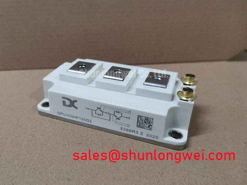
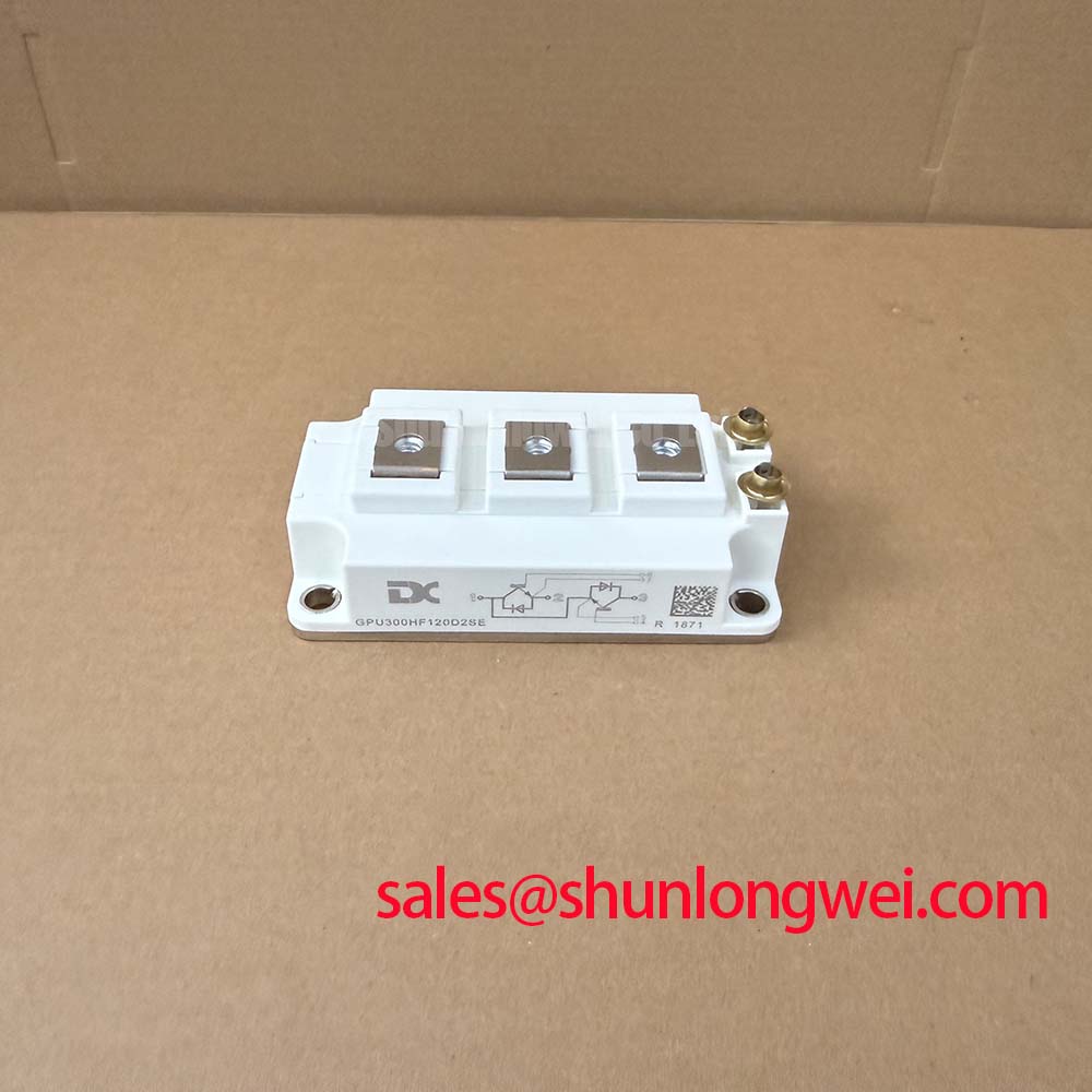
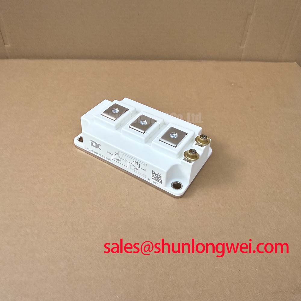
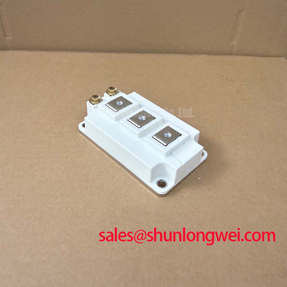
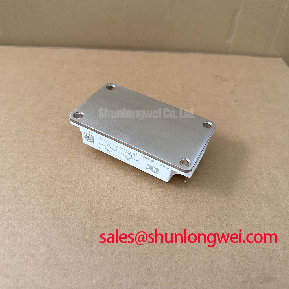
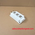
Before installation, isolate the module and verify the marked power terminals against the original inverter schematic, then record the cold-state diode-mode readings and package condition for comparison with a known-good unit. The GPU300HF120D2SE from MacMic is a high-current IGBT module specified for a 1200 V collector-emitter blocking voltage and a 300 A continuous DC collector current at TC = 80°C. These are official datasheet specifications, not system-level operating guarantees.
The module uses a 62 mm standard housing with a three-screw dual-pack construction. Its listed typical collector-emitter saturation voltage is 2.30 V, while the gate-emitter maximum rating is ±20 V. The official input capacitance value is 22.0 nF. Gate-driver voltage, switching frequency, gate resistance, thermal resistance, short-circuit capability, and transient limits must be confirmed from the applicable manufacturer documentation before a replacement design is released.
| Parameter | Official Value | Engineering Identity |
|---|---|---|
| Collector-emitter voltage | 1200 V | Official Datasheet Specification |
| Continuous DC collector current at TC = 80°C | 300 A | Official Datasheet Specification |
| Typical collector-emitter saturation voltage | 2.30 V | Official Datasheet Specification |
| Gate-emitter maximum rating | ±20 V | Official Datasheet Specification |
| Input capacitance | 22.0 nF | Official Datasheet Specification |
| Housing geometry | 62 mm standard, three-screw dual pack | Official Datasheet Specification |
For a commercial string inverter or micro-grid energy-storage converter, the 1200 V rating should be treated as a component boundary that requires system-level voltage headroom assessment. The DC bus can experience overshoot during regenerative events, emergency shutdown, capacitor-bank switching, and control-loop faults. Designers should measure the actual collector-emitter waveform at the module terminals rather than judging compatibility from nominal bus voltage alone.
Altitude and terrestrial neutron exposure can be relevant reliability considerations for high-voltage power semiconductors, particularly above 2000 m. However, no FIT value, Single Event Burnout rate, or altitude derating curve is established by the supplied product data. Any SEB assessment should therefore use a qualified manufacturer application note, an accredited test report, or a recognized reliability methodology. Without that source, the responsible engineering action is to verify peak voltage, switching duration, repetitive stress, enclosure cooling, and protection response under the intended installation conditions.
Maintain the original creepage and clearance arrangement around the high-voltage terminals, especially where contamination, condensation, or dust may reduce insulation performance. The module’s package geometry does not by itself define the final system insulation distance. The equipment designer must evaluate working voltage, pollution environment, material group, altitude, and applicable insulation standard.
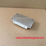
During incoming inspection, check the screw-hole area for cracks, terminal deformation, contamination, or evidence of mechanical stress. Confirm that the mounting surface is flat and clean, and apply the thermal interface method specified by the equipment manufacturer. Bench Tip: keep the module protected against ESD and compare all cold-state measurements with a known-good reference before applying gate-drive power.
Protection Coordination and Parallel Current Sharing
The listed typical 2.30 V VCE(sat) is useful when reviewing conduction loss, but it should not be converted directly into a complete thermal design. Actual loss depends on collector current, junction temperature, switching conditions, gate-drive behavior, and the manufacturer’s test conditions. When checking a failed inverter board, measure the collector-emitter voltage under controlled current and compare it with the original operating waveform rather than using a single handheld-meter reading as a pass or fail decision.
IGBTs operated in parallel require matched electrical paths. The positive temperature coefficient commonly associated with IGBT saturation voltage can support static current sharing, but dynamic sharing is strongly affected by gate-loop inductance, driver timing, stray capacitance, emitter impedance, and busbar symmetry. This is a Design Consideration, not a guaranteed characteristic for every operating point of this module. Designers should keep corresponding gate and emitter paths physically similar and confirm current balance with isolated probes or other suitable measurement equipment.
The official data supplied here does not include gate charge Qg, gate-drive current, recommended gate resistance, or switching energy. Consequently, bootstrap capacitor sizing cannot be assigned a valid fixed value from the available information. As an Engineering Recommendation, the design calculation should account for the gate charge delivered during each switching event, driver quiescent consumption, leakage, bootstrap diode behavior, refresh interval, temperature, and allowable gate-voltage droop. The resulting value must then be validated at the actual duty cycle and switching frequency.
High-side isolation also deserves attention in industrial drive boards. An optocoupler or digital isolator must be selected according to the required common-mode transient immunity, propagation delay, fault behavior, and isolation rating. The general operating principle of galvanically isolated gate-drive signaling is described in Galvanically Isolated Optical Couplers for Gate Drive Signals. The system integrator should verify the driver supply voltage from the original control-board documentation rather than assuming a universal value.
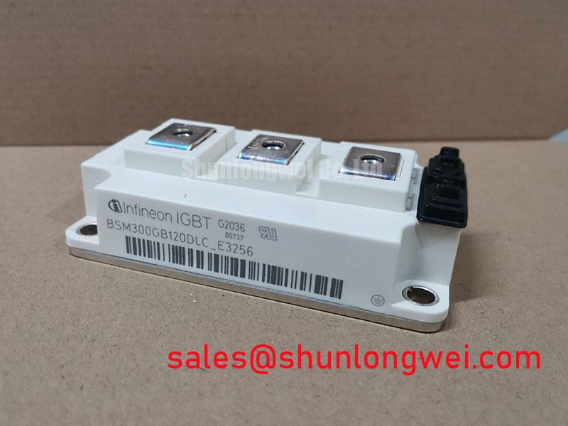
In a replacement evaluation, MBM200JS12EW may be reviewed as a separate, objectively specified IGBT module for comparison. Electrical interchangeability still depends on terminal arrangement, electrical ratings, switching data, thermal interface, and the gate-driver design.
DC-Link Capacitance Bank and Switching Overshoot Control
The DC-link capacitor bank should be placed and connected so that the high-current commutation loop is as compact and symmetrical as the equipment architecture permits. During turn-off, stray inductance and current slew can raise the collector-emitter peak above the measured DC-link voltage. The engineering relationship is commonly expressed as the DC voltage plus the inductive contribution from stray inductance and current change rate. This is a calculation aid, not a guaranteed limit for the GPU300HF120D2SE.
Use a differential high-voltage probe with an appropriate bandwidth and connection method when checking overshoot. Probe ground leads, busbar joints, laminated-bus transitions, capacitor mounting tabs, and fuse connections can introduce measurement artifacts or additional inductance. The design target for loop inductance must be established by the system engineer from the measured switching waveform, device voltage rating, clamp behavior, and required transient margin; a fixed layout number should not be assigned without the complete topology and test conditions.
Snubbers, active clamps, and local film capacitors should be evaluated only after the switching node has been measured. Snubber capacitance is determined by the permitted voltage excursion, switching energy, pulse repetition, damping resistance, capacitor pulse capability, and thermal loss. Increasing capacitance without checking turn-on current and control-loop effects can create a different stress condition. For regenerative braking systems, the brake chopper and resistor bank must also be checked for peak pulse energy, average dissipation, switching coordination, and DC-link fault response.
The front-end topology may include a rectifier or auxiliary power stage such as K420A4001. That association does not establish a substitute circuit or compatibility claim. Engineers should verify the complete power path, including precharge, fusing, contactor timing, capacitor ripple current, and protection coordination.
Benchtop Waveform Tuning and Emitter Return Control
When the package and schematic provide a dedicated auxiliary or Kelvin emitter connection, route the gate-driver return separately from the main high-current emitter path. Shared copper can introduce mutual coupling and emitter voltage movement, which may alter the effective gate voltage during fast transitions and contribute to ringing or false protection trips. The presence and exact terminal identity must be verified from the original package drawing; it should not be inferred from the model number alone.
At the bench, first confirm gate-to-emitter polarity and inspect the gate waveform with a short, controlled probe connection. Check turn-on and turn-off behavior at reduced test energy before connecting the full DC-link source. If oscillation appears, compare the gate signal at the driver output with the signal measured directly at the module terminals. This can help distinguish driver-path impedance, measurement-loop pickup, common-emitter coupling, and power-loop overshoot without assigning one symptom to one cause.
The ±20 V VGES rating is an absolute maximum specification, not a recommended operating command. Gate-voltage clamp selection, negative bias, Miller control, dead time, and desaturation response remain system-design decisions. The module’s 22.0 nF Cies value indicates a significant driver loading consideration, but it does not replace a full gate-charge and switching-loss evaluation.
Gate insulation must be protected from excessive transient voltage, contamination, and uncontrolled driver startup. Quantum tunneling is a recognized physical mechanism in ultra-thin dielectric breakdown, as outlined in Quantum Tunneling in Ultra-Thin Dielectric Gate Breakdown; this reference should not be interpreted as a failure-rate prediction for this specific module. For broader context on wide-bandgap devices and their system-level design challenges, engineers can consult Wide Bandgap Revolution.
After assembly, verify gate polarity, isolation, terminal torque according to the equipment manufacturer’s instructions, thermal contact, DC-link precharge, and oscilloscope waveforms during controlled switching tests. Confirm the measured collector-emitter peak remains within the system-approved voltage envelope and that protection circuits respond before the module’s official electrical boundaries are approached.