Content last revised on September 3, 2026
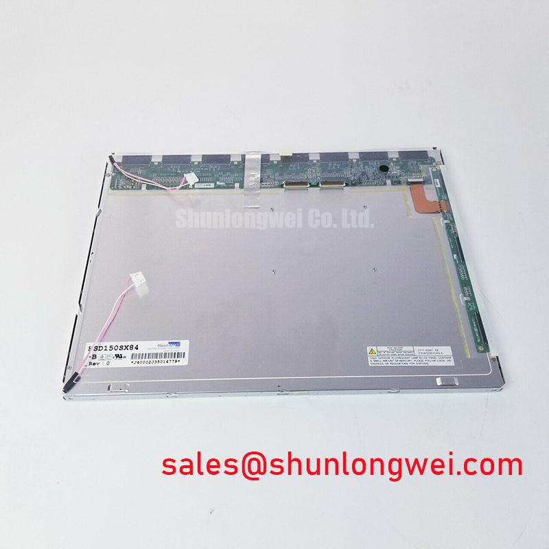
Incoming bench inspection of the HannStar HSD150SX84-C03 begins with measuring unpowered logic rail pin-to-ground resistance across the interface connector, verifying continuity across the chassis perimeter ground tabs, and inspecting the outer bezel for mechanical planar deflection. In rugged human-machine interface retrofits, such as an Automated Guided Vehicle (AGV) & Forklift Rugged Telematics Display subjected to continuous vibration and fluctuating DC bus voltages, verifying physical tolerances and electrical boundaries prior to assembly ensures the display module functions reliably under industrial field conditions.
High-Nits Edge-Lit LED Rail Thermal Dissipation & PMMA Light Guide Plate Preservation
Thermal management of the HannStar HSD150SX84-C03 edge-lit LED backlight architecture requires balancing luminance output against internal thermal accumulation. In high-ambient outdoor or industrial cabin environments, driving backlight LEDs at sustained peak forward currents creates localized heat concentrations along the module edge where the LED rail mounts. Without an adequate heat-sinking path, this thermal energy transfers directly into the adjacent Poly(methyl methacrylate) (PMMA) light guide plate (LGP). PMMA exhibits a non-trivial coefficient of thermal expansion and undergoes accelerated polymer chain degradation when subjected to continuous elevated temperatures. Over extended deployment cycles, thermal concentration along the edge induces localized optical yellowing, visible luminance non-uniformity across the bottom edge, and permanent warping of the light guide substrate.
To preserve optical clarity and ensure backlight operational longevity consistent with industrial L70/B50 standards (where luminance retains 70% of initial output across rated operating hours), system integrators must mechanically couple the panel's rear aluminum bezel to the system enclosure using thermally conductive interface materials. Sizing an extruded aluminum heat spreader rail directly along the edge-lit assembly draws heat away from the LED printed circuit strip, spreading thermal dissipation across the entire chassis mass. When evaluating operating envelopes, system designers should establish thermal boundaries that keep internal junction temperatures below the LED manufacturer's derating threshold during maximum ambient conditions.
Backlight driving circuits must implement robust diagnostic and protection loops, including open-circuit detection, individual LED string short-circuit sensing, and feedback-controlled overvoltage clamping. If an individual LED string fractures due to mechanical shock, the constant-current driver must promptly detect the impedance drop or open loop, terminating drive current to prevent overvoltage stress on adjacent channels. Furthermore, brightness modulation requires careful design consideration: pulse-width modulation (PWM) dimming frequencies must be selected between 200 Hz and 1 kHz. Maintaining the switching frequency above 200 Hz eliminates visible optical flicker and stroboscopic effects during operator eye movement, while keeping it below 1 kHz prevents excessive switching losses and audible acoustic resonance within the driver's ceramic decoupling capacitors and inductive chokes.
Cold-ambient operational profiles present the inverse physical challenge. As operating temperatures drop toward sub-zero ranges (-20°C to -30°C), the kinematic viscosity of the nematic liquid crystal fluid inside the panel cell escalates exponentially. This fluid stiffening impairs the electrostatic reorientation of the liquid crystal molecules between off and on states, elongating Gray-to-Gray (GTG) response times from nominal millisecond ratings to several hundred milliseconds, which manifests on screen as visible image ghosting and smearing during graphic updates. To mitigate this effect in cold-storage warehousing or outdoor telematics systems, integrators frequently evaluate transparent resistive ITO heating glass or rear-mounted silicone heating mats. Controlled via external thermal sensing circuits, these auxiliary heating elements pre-condition the liquid crystal cell until core operating temperatures reach the normal dynamic response envelope.
Industrial EMI Noise Immunity, Chassis Shielding Continuity & Common-Mode Ferrite Chokes
Deploying the HannStar HSD150SX84-C03 display module in proximity to heavy inductive switching elements, such as 400V variable frequency drives (VFDs), forklift traction inverters, or electromechanical hydraulic contactors, introduces intense high-frequency electromagnetic interference (EMI). Fast transient switching edges ($dv/dt$ and $di/dt$) couple onto floating metal structures and unshielded cable harnesses via capacitive and inductive cross-talk. If common-mode ground return currents traverse the display's internal ground planes, the resulting ground bounce corrupts low-voltage differential signaling thresholds, triggering horizontal white noise bands, intermittent frame loss, or complete graphic controller freeze-ups.
Ensuring robust noise immunity requires continuous, low-impedance grounding across the entire mechanical stack. The perimeter sheet metal frame of the HSD150SX84-C03 serves both as structural support and as a Faradaic shield for the internal Timing Controller (T-CON) and row/column source drivers. When installing the module into an enclosure, the mounting brackets must establish clean metal-to-metal contact with the system chassis. Anodized coatings, non-conductive powder paints, or adhesive films must be cleared at mounting touchpoints, or bridged using conductive beryllium copper gaskets or silver-loaded elastomer strips to provide a multi-point RF sink to chassis ground.
Interconnect cabling between the main host single-board computer (SBC) and the panel's LVDS connector represents the most vulnerable path for electromagnetic ingress. Integrators should implement 360-degree shielded twisted-pair wire harnesses or shielded flat flexible cables (FFC) featuring an integrated vapor-deposited aluminum-mylar shield or silver foil wrap. The cable shield must terminate directly to the metal backshell of the interface connector, bonding directly to the chassis ground plane at both terminal ends rather than being drained through a narrow pigtail wire, which introduces parasitic inductance and destroys RF shielding performance at frequencies above 30 MHz.
⚠️ Field Alert: Disconnect all incoming system power supplies and discharge DC-link filter banks before mating or unseating the panel interface harness to prevent contact misalignment from triggering destructive latch-up inside the sensitive T-CON receiver.
Where high common-mode currents exist along the cable run, snap-on or overmolded common-mode ferrite chokes should be placed directly adjacent to the display module connector. Selecting a broadband NiZn ferrite core provides high common-mode impedance across the 30 MHz to 300 MHz band, attenuating radiated energy coupled from high-power PWM switching circuits without degrading the balanced odd and even differential signal modes traveling along the interior signal conductor pairs.
Controlled 100-Ohm Differential Impedance Flex Routing to Suppress High-Frequency Jitter
The transmission of high-resolution graphic data to the HannStar HSD150SX84-C03 relies on Low-Voltage Differential Signaling (LVDS). Operating with a nominal differential voltage swing around 350 mV over a balanced 1.2V common-mode baseline, LVDS offers low radiated emissions and high noise immunity, provided physical routing rules are rigorously maintained. Maintaining signal integrity requires precise PCB transmission line engineering, demanding a target 100-ohm differential characteristic impedance (typically ±10% tolerance) across the entire link, encompassing the host controller board, connecting flex cables, and transitional interface connectors.
Impedance discontinuities along the differential traces cause high-frequency reflections that degrade eye-diagram openings at the panel's T-CON receiver inputs. Reflections manifest as excessive phase jitter on the differential pixel clock pair, narrowing receiver setup and hold margins. When jitter exceeds internal phase-locked loop (PLL) tracking limits, the receiver incorrectly decodes incoming serial pixel bits, resulting in sparkler artifacts, color shifting, or line-synchronization failures.
💡 Pro Tip: Route LVDS differential pairs with strictly matched intra-pair lengths and continuous reference planes to minimize skew-induced phase jitter on the pixel clock receiver.
Power sequencing parameters govern long-term semiconductor reliability inside the integrated display electronics. The logic supply voltage (nominally 3.3V or specified panel VDD) must observe controlled rise-time characteristics during initialization. If the power-on ramp time ($t_1$) rises too slowly (e.g., exceeding 10 ms to 20 ms), internal logic gates may linger in indeterminate states, inducing excessive shoot-through currents that trigger core latch-up. Conversely, an excessively steep supply ramp rate ($t_1 < 0.5$ ms) can induce high inrush currents across decoupling capacitors, dropping the upstream power supply rail out of regulation.
Equally critical is the sequencing interval between logic power stabilization and data signal assertion. System software must ensure valid differential clock and data signals are applied only after the logic rail has reached stable operating regulation, followed by an intentional delay before turning on the backlight inverter or LED constant-current driver. Disabling power follows the reverse sequence: turn off the backlight first, cease LVDS transmission second, and collapse logic VDD last. Violating this sequence forces high-frequency signals into unpowered CMOS receiver inputs, turning on internal ESD parasitic diodes and causing structural oxide degradation over time.
| Parameter / Design Domain | Engineering Specification / Boundary Criteria | Physical Verification & Operational Impact |
|---|---|---|
| Transmission Line Impedance | 100 Ω ±10% differential impedance | Design Consideration: Prevents signal reflections and maintains eye-pattern opening at T-CON. |
| Logic Supply Ramp ($t_1$) | 0.5 ms < $t_1$ < 10 ms (Standard Logic Envelope) | Official Specification: Eliminates high inrush surges while preventing CMOS intermediate state latch-up. |
| Data Mapping Alignment | JEIDA vs. VESA 6-bit / 8-bit matching | System Requirement: Misalignment causes severe solarization, contour banding, or false colors. |
| Backlight PWM Frequency | 200 Hz to 1.0 kHz modulation range | Design Consideration: Suppresses optical flicker and prevents audible ceramic capacitor resonance. |
Optical performance under harsh lighting conditions also depends on proper alignment between the graphic data map and the panel. Misinterpreting JEIDA and VESA transmission formats in system software shifts color data packets relative to control bits, causing intense solarization or banding artifacts across the display. In outdoor environments under direct ambient solar loading (often exceeding 50,000 lux), maintaining readable contrast requires a panel fitted with an anti-glare (AG) surface finish with hard-coating properties. The AG surface structure breaks up direct specular mirror reflections into diffuse patterns, maintaining acceptable contrast and preventing visual obscuration without altering native liquid crystal polarization.
High-Humidity Storage Margins (60°C / 90% RH) & Delamination Prevention Protocols
Industrial storage and field operation subject display hardware to extreme climatic conditions, where elevated temperature and relative humidity combine to challenge the chemical and physical integrity of the panel stack. Extended exposure to 60°C ambient temperatures at 90% relative humidity (RH) tests the hermetic integrity of the module's perimeter epoxy seals. Water vapor molecules, possessing a small kinetic diameter, can gradually permeate microscopic imperfections in organic adhesives. If moisture penetrates the liquid crystal cell, it disrupts the polar alignment of the liquid crystal molecules, creating permanent dark patches, localized clearing point degradation, and visible resistive path leakage across the transparent ITO matrix.
For comprehensive guidelines covering optical bonding techniques, thermal mitigation architectures, and environmental qualification standards across harsh installations, review The Ultimate Guide to Industrial TFT LCD Technology.
Mechanical stress accelerates environmental failure modes when the display panel is mounted within rigid, non-compliant chassis bezels. The HannStar HSD150SX84-C03 assembly contains multiple layers of bonded materials—including front and rear linear polarizers, color filters, TFT glass substrates, and optical brightness enhancement films (BEF)—each possessing distinct thermal expansion coefficients. Rapid thermal cycling across industrial operational limits (-30°C to +85°C) generates continuous shear stresses along the adhesive interfaces.
When mechanical mounting clamps exert excessive localized clamping forces or uneven torsional torque on the outer bezel, these internal shear stresses multiply. Uneven mechanical compression forces the thin glass substrates inward, altering the cell gap spacing between the front and rear polarizers. A cell gap change of mere fractions of a micrometer alters the optical phase retardation of polarized light, producing visible yellow or white light pooling (mura effects), particularly noticeable across dark backgrounds. Under severe, sustained thermal-mechanical stress, this localized pressure causes permanent delamination of the polarizer film from the glass substrate, allowing ambient moisture to condense within the resulting voids.
Preventing mechanical stress-induced optical defects requires compliant mounting methodologies. Enclosure bezels must incorporate continuous, closed-cell elastomeric gaskets (such as high-grade EPDM or fluorosilicone foam) that absorb enclosure flexing and distribute clamping force evenly along the perimeter frame. Direct point contact from rigid metal bosses against the active display borders must be strictly avoided. Enclosure cutouts should allow clearance for thermal expansion across the maximum operational temperature range, ensuring that the HannStar HSD150SX84-C03 retains mechanical compliance, environmental seal integrity, and stable optical output throughout its operating life.