Content last revised on September 17, 2026
Field Diagnostics & Commissioning: Optimizing Gate Drive Loop Geometry in IRS21531DSTRPBF Topologies
With power removed and the DC link discharged, inspect the IRS21531DSTRPBF solder joints, supply decoupling path, bootstrap network, and HO/LO gate-drive traces before applying power. This Infineon half-bridge gate-driver IC is specified for a maximum 600 V offset voltage, a 1.2 us typical internal deadtime, a 15.6 V typical VCC clamp voltage, 150 uA typical startup current, and plus or minus 400 mA peak output current. Its SOIC-8 package supports compact surface-mount control boards where trace routing often determines whether a repaired inverter starts cleanly or shows gate ringing.
The driver itself has no Kelvin-emitter terminal. In a half-bridge using external MOSFETs or IGBTs, the relevant design consideration is to keep each gate-drive return referenced to the associated power-switch source or emitter as directly as the PCB topology permits. Avoid sharing a long, high-current power-return section with the driver return. Shared inductance can translate switching current changes into apparent gate-voltage movement, which may produce oscillation or unexpected switching behavior. During commissioning, compare the gate-to-source or gate-to-emitter waveform with the switching-node waveform using measurement methods appropriate to the circuit and probe arrangement.
| Official Specification | IRS21531DSTRPBF Value | Integration Relevance |
|---|---|---|
| Offset voltage | 600 V maximum | Defines the high-side switching offset boundary. |
| Internal deadtime | 1.2 us typical | Provides non-overlap timing between the half-bridge outputs. |
| Output peak current | plus or minus 400 mA | Establishes the output-drive capability for the external gate network. |
| Startup current | 150 uA typical | Relevant to startup-path and bootstrap-support assessment. |
| Package | SOIC-8 | Requires footprint, soldering, and creepage review at board level. |
For a repair assessment, verify that the board's intended gate resistor, bootstrap capacitor, bootstrap diode, and supply bypass components remain connected to the correct pins and that there is no conductive contamination around the package. The 15.6 V typical VCC clamp is an official device characteristic, not a substitute for validating the upstream supply during abnormal operating conditions. Engineers should measure the supply rail and high-side bootstrap behavior against the original equipment documentation before treating a driver issue as the primary fault.
Safety note: Discharge and verify the DC-link voltage before probing, reworking, or reconnecting any half-bridge control-board wiring.
Benchtop Waveform Tuning: Preventing Overvoltage Stress During Fast Switching
Bring up a repaired board first with the control signals, supply rail, and switching-node behavior under observation, then validate operation within the equipment's approved test arrangement. The IRS21531DSTRPBF supplies complementary half-bridge drive with its 1.2 us typical internal deadtime; it does not measure DC-link voltage, control a braking resistor, or provide a specified regenerative-braking function. Any braking transistor, braking IGBT, ballast resistor, motor, and DC-link capacitor bank belong to the surrounding power system and must be assessed from that system's documented ratings.
In motor-control equipment, deceleration energy can increase DC-link stress when the load returns energy to the bus. As an engineering consideration, validate the braking path, DC-link sensing method, and thermal path as a complete subsystem, particularly after a control-board repair. A failed braking circuit, altered motor-command behavior, or inadequate energy absorption can all contribute to elevated bus voltage; waveform evidence and the original system schematic are needed to distinguish among them.
Fast-switching transitions are also influenced by the reverse-recovery behavior of the selected freewheeling diode or body-diode path, external gate resistance, driver-loop geometry, and DC-link placement. Ringing observed at the switching node may indicate a combination of parasitic inductance, component behavior, and measurement-loop pickup. A practical recommendation is to minimize the physical loop area between the local DC-link capacitors and the switching pair, then verify peak voltage margins during representative switching tests. The relationship between bus voltage, loop inductance, and current-transition rate explains why a physically distant capacitor can worsen overshoot even when its nominal capacitance appears adequate.
For external MOSFET selection or review, Infineon's OptiMOS low-voltage MOSFET portfolio and its broader OptiMOS and CoolMOS power MOSFET information provide technology context. Compatibility remains system-dependent: the integrator should verify voltage rating, gate-charge behavior, thermal conditions, topology, and switching measurements rather than infer suitability from a device family name.
IRS21531DSTRPBF Circuit Protection & Reliability: Establishing Verified Operating Boundaries
The 600 V maximum offset-voltage specification is the primary official high-side boundary to preserve when evaluating an IRS21531DSTRPBF installation. It should not be interpreted as a complete inverter voltage-survivability rating because switching-node overshoot, supply behavior, external power-device capability, layout, and transient conditions are determined by the assembled system. Engineers should capture the relevant waveforms and compare them with the documented limits of every device in the power path.
There is no provided official FIT rate, single-event burnout rate, altitude qualification, cosmic-ray rating, or operating-life figure in the supplied product data. Those reliability subjects therefore require engineering consideration rather than a numerical claim for this IC. Equipment intended for elevated-altitude operation should be evaluated under the applicable system safety, insulation, thermal, and electrical-transient requirements by the responsible system engineer. No specific failure-rate projection can be made from the listed gate-driver parameters.
Miller-induced turn-on is a board-level risk when a fast-changing switching node couples through the external power switch's gate-drain capacitance. The IRS21531DSTRPBF's output arrangement must be evaluated with the chosen external switch, gate network, and return routing. Designers should verify that the inactive switch remains controlled during the opposing device's transition and should use measured gate waveforms to assess the effectiveness of the chosen damping and bias arrangement. For circuit-level discussion of off-state gate-bias approaches, see Evolution of Negative Off-Bias Gate Drive Circuits; the required bias strategy, if any, is determined by the external power-switch datasheet and system tests.
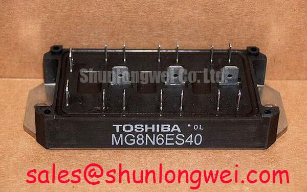
In a board repair involving a separate power module, BSM100GAL100D is a distinct power-semiconductor module that can be reviewed as part of the wider power-stage bill of materials. It is not an interchangeable replacement for the SOIC-8 IRS21531DSTRPBF gate-driver IC. Confirm the function, package, pinout, electrical ratings, and original circuit role before selecting any replacement component.
Preventing Spurious Faults: DC-Link Capacitor Bank Layout and Low-ESR Verification
Inspect the local DC-link capacitor bank, high-current copper paths, and gate-driver supply bypassing as separate but interacting circuits. The IRS21531DSTRPBF has plus or minus 400 mA peak gate-drive outputs, so its short switching pulses charge and discharge the external power switches' gate capacitances while the power stage moves much higher load current elsewhere. A common repair error is to focus only on the IC while overlooking cracked capacitors, lifted copper, degraded solder joints, or altered return paths near the half bridge.
As an engineering consideration, reduce parasitic inductance in the commutation loop to suppress turn-off overshoot, and verify the resulting peak voltage against the DC-link level with appropriate switching tests. This should be achieved through compact capacitor-to-switch routing and balanced current geometry, not by assuming one layout rule applies to every board. Snubber components, where used, require validation against the actual oscillation frequency, thermal loading, and voltage stress observed in the target equipment.
Spurious shutdowns or erratic switching can arise from more than one source, including supply disturbance, incorrect bootstrap charging conditions, noise coupled into input signals, an unstable gate loop, or a power-stage defect. Inspect the VCC rail, input timing, LO output, HO output, and switching node in a controlled sequence, comparing results with a known-good signal path or original documentation where available. The 150 uA typical startup current is useful when reviewing the intended startup arrangement, but it does not define the behavior of an entire auxiliary supply.
In forklift traction-controller servicing, an auxiliary rectifier or power-stage component such as P950A may appear elsewhere in the converter architecture. Its role and suitability must be verified from the actual schematic and device documentation. Treat the IRS21531DSTRPBF as the half-bridge driver specified by its own official ratings, then validate its interaction with the surrounding DC-link, bootstrap, input-control, and external switching circuits.