

Content last revised on October 15, 2026
Dynamic Contrast Ratio Stabilization and Liquid Crystal Birefringence Temperature Tracking
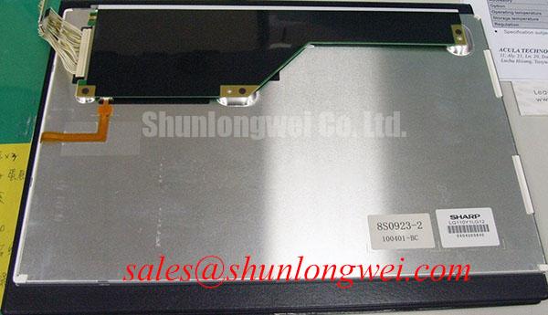
When a replacement panel produces washed highlights, grayscale inversion, or uneven viewing performance, first compare the image at normal viewing position and at oblique angles while the display reaches its operating temperature. The LQ110Y3DG01 is a Sharp TFT LCD active matrix color display module listed as an industrial grade LCD and HMI panel in a decoded baseline standard form factor.
The supplied product baseline does not assign a confirmed panel architecture, viewing cone, contrast ratio, anti glare treatment, or sunlight performance value to this model. Those characteristics should therefore be assessed from the original panel documentation and from the installed unit rather than inferred from the model number. TN, IPS, and MVA panels can show different grayscale behavior as the viewing angle and liquid crystal temperature change, so a visual comparison should use identical test images, identical backlight settings, and the same observation angle.
For equipment exposed to strong ambient illumination, inspect dark screen uniformity and highlight detail under the actual enclosure lighting. A contrast result above 500:1 at 50,000 lux must not be presented as an LQ110Y3DG01 factory specification unless it is stated in the applicable Sharp datasheet or test report. It is a system level optical acceptance target only when the equipment designer defines it for the application. Surface anti glare treatment can reduce reflected hotspots, but the final result also depends on cover glass, bezel depth, ambient light direction, and display calibration.
Temperature tracking is equally important during incoming inspection. Display a stepped grayscale pattern after cold start, then repeat the observation after thermal stabilization. Changes in black level, shadow detail, or color balance can point to panel temperature behavior, backlight regulation, source timing, or the host image chain. Record the observation without assigning a failure to the panel until the cable, controller, and supply conditions have been checked.
Sharp’s industrial display resources provide useful context for optical integration and application requirements through Sharp Devices Europe Industrial Display Solutions and the Sharp Display Solutions Official Portal. These resources should be treated as manufacturer information sources, not as confirmation that every listed characteristic applies to this specific model.
Constant Luminance Output Control and Backlight Lifetime Reliability Verification
Check luminance across the active area rather than relying on a single center point when evaluating a replacement LQ110Y3DG01 in an HMI or medical imaging display. Edge darkening, localized bright regions, and color temperature drift can originate from the backlight assembly, mechanical pressure, optical stack alignment, or the host brightness control.
The available baseline identifies the part as a TFT LCD active matrix color display module, but it does not provide a confirmed LED lifetime, L70 or B50 value, backlight current, luminance rating, or thermal rail construction. These figures must not be assigned to the model without the corresponding factory documentation. A practical incoming inspection can still compare center and edge luminance, white point consistency, startup behavior, and visible response after the display has been operating under the intended enclosure conditions.
Where the equipment uses narrow aluminum heat spreader rails or another chassis heat path, treat them as system design features rather than as confirmed parts of this panel. The mechanical design should distribute heat without placing concentrated pressure on the bezel or active area. Thermal contact, ventilation, enclosure sealing, and nearby electronics can influence the backlight temperature. The system engineer should validate any L70 or B50 claim against the actual drive current, duty cycle, ambient temperature, and optical acceptance limit.
| Evaluation item | LQ110Y3DG01 | NL6448BC28 01 |
|---|---|---|
| Manufacturer | Sharp | Confirm from product documentation |
| Product category | Industrial grade LCD and HMI panel | LCD display module for comparative evaluation |
| Construction description | TFT LCD active matrix color display module | Confirm from product documentation |
| Baseline status | Decoded baseline and standard form factor | Confirm mechanical and electrical compatibility |
| Replacement assessment | Reference unit under evaluation | NL6448BC28 01 for neutral side by side assessment |
This comparison is a screening aid, not a substitute for checking outline dimensions, mounting points, connector position, pin assignment, display timing, backlight wiring, and controller compatibility. A mechanically similar panel can still produce a blank image, incorrect colors, or unstable startup when its host interface differs.
Clock stability and data hold behavior should be measured at the panel connector when the host uses TTL or LVDS signaling. The acceptable timing window belongs to the complete transmitter, cable, receiver, and temperature range. An oscilloscope or suitable high speed probe can reveal edge distortion and timing movement that a static image test will miss. Do not convert an L70 or B50 industry term into a guaranteed service life for this model without a source specific test condition.
💡 Bench Tip: Disconnect power before handling the display cable, use ESD protection, and press the flexible cable squarely into the connector before locking it.
Suppressing Pixel Jitter and Horizontal White Lines Induced by Adjacent 400V Motor Drives
Separate the display signal path from switching power conductors when pixel jitter or horizontal white bands appear near a variable frequency motor drive. The 400 V motor drive is an application example, not a stated operating condition of the LQ110Y3DG01. Noise can enter through cable coupling, connector reference movement, supply disturbance, or an unsuitable controller layout.
Begin by comparing the panel with the motor drive disabled and then enabled under the same image pattern. Observe whether the disturbance follows motor speed, switching state, cable position, or enclosure door position. This controlled comparison helps distinguish radiated coupling from conducted interference without assigning a single cause to the panel. Review the shield termination and signal return path at both the display and controller ends according to the equipment EMC design.
A fully surrounded shield or shielded FFC arrangement can reduce electric field coupling when the shield is continuous and bonded correctly. It is not automatically effective if the shield has a long pigtail, an interrupted reference, or an unsuitable chassis connection. Common mode ferrite components may be considered by the system designer where measurements show common mode energy, but their impedance behavior must be evaluated across the signal spectrum and operating temperature.
For LVDS systems, inspect differential pair symmetry, pair spacing, reference continuity, and connector seating. For TTL systems, examine parallel data transitions, clock edge quality, and return current paths. The model baseline supplied for this page does not confirm a TTL or LVDS interface for LQ110Y3DG01, so the original panel pinout and controller documentation must determine which measurement method applies.
When a white line appears only during switching events, capture the display supply and interface activity at the same time. A disturbance on the logic rail, a shifted clock edge, or a transient reference movement can create similar visible symptoms. Verify the known good signal path before changing cable shielding or adding filtering. EMC acceptance remains a property of the assembled equipment; the LCD module alone should not be described as independently certified to a system EMC standard.
For long operating periods, use a stable image pattern and periodically inspect uniform gray fields, fine text, and horizontal gradients. The supporting technical background in The Ultimate Guide to Industrial TFT LCD Technology can help engineers relate panel construction, signal integrity, and application selection without treating general principles as model specific ratings.
TTL 24 Bit Digital RGB Bus Synchronization and Logic Power Rail Verification
Confirm the host bus format before applying power to an LQ110Y3DG01 replacement panel, because a connector that fits mechanically does not establish pin compatibility. The supplied baseline confirms the product category and TFT LCD active matrix construction, but it does not publish a verified logic voltage, TTL 24 bit mapping, LVDS assignment, power on rise time, PWM input, or backlight control specification.
Where the original system uses a TTL 24 bit RGB bus, inspect the pixel clock, data enable, synchronization signals, and color bit order at the panel connector. JEIDA and VESA mapping conventions are not interchangeable assumptions; the controller configuration must match the panel documentation. Incorrect mapping can produce split images, swapped color significance, unstable synchronization, or a partially active screen even when the panel illuminates.
Power sequencing deserves attention during a white screen or residual image investigation. The system integrator should verify the required supply voltage from the original panel documentation, then measure the rail rise, reset behavior, enable order, and discharge condition during power removal. The proposed 0.5 ms to 10 ms rise window is a design requirement from the supplied integration brief, not a confirmed factory rating for this Sharp model. Use it only when the host system specification calls for that window and validate the result at the panel connector.
A nominal rail reading taken after startup can conceal a poor power on event. Capture the rail and display enable together, check for overshoot or repeated restart behavior, and compare a cold start with a warm restart. White screen behavior can also result from absent timing, incorrect reset state, or a locked controller, so the diagnostic sequence should include the signal activity and not only the supply measurement.
For differential interfaces, a nominal 100 ohm differential characteristic impedance is a common routing objective, but the actual target must follow the selected transceiver and panel interface documentation. Keep the route continuous, control pair geometry through transitions, and avoid unnecessary stubs. For TTL wiring, prioritize short parallel paths, a clean return reference, and controlled edge behavior. These are design considerations for the complete assembly rather than LQ110Y3DG01 factory specifications.
PWM brightness control also requires system validation. The integration brief identifies 200 Hz to 1 kHz as a possible design range for evaluating flicker, audible interaction, and duty cycle linearity. It must not be presented as a confirmed input range for this panel without source documentation. If the original unit uses PWM, compare brightness steps with a photometer and inspect low duty operation for visible modulation. If the panel uses another backlight control method, retain the original control architecture instead of applying an assumed PWM signal.
During final installation, inspect FPC bend radius, connector latch engagement, bezel clearance, and chassis stress after the display is fastened. A rigid mounting point can transfer vibration or enclosure distortion into the glass and cable interface. Cold starts, static interface pages, and repeated power cycles should be included in the equipment acceptance plan, with results recorded against the original display behavior and the manufacturer’s applicable documentation.