

Content last revised on September 18, 2026
Assembly Integrity & Layout Architecture: Minimizing Commutation Turn-Off Voltage Stress for MCC40 16I06
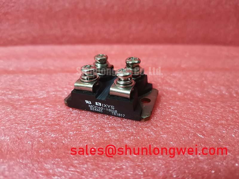
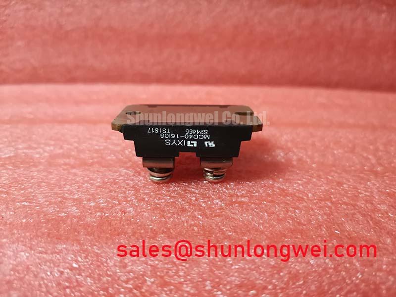
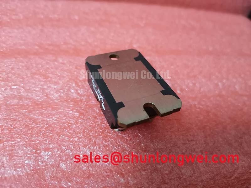
Before connecting the power circuit, inspect the module housing, terminal areas, mounting face, and nameplate, then confirm that the installed device is MCC40 16I06 and that its marked electrical boundary matches 1600V and 40A. These are Official Datasheet Specifications for this IXYS module. A cold equipment check should begin with the original schematic and terminal identification from the applicable manufacturer documentation, because a dual thyristor module must be connected according to the intended bridge, AC controller, or capacitor switching topology.
| Item | Declared value | Status |
|---|---|---|
| Manufacturer | IXYS | Product identification |
| Device type | Dual Thyristor Module | Product category |
| Voltage rating | 1600V | Official Datasheet Specification |
| Current rating | 40A | Official Datasheet Specification |
| Package | Module | Official package description |
For an incoming inspection, isolate the assembly from the energized system and use the diode test function only as a comparative cold test between corresponding terminal paths on a known good circuit position. Thyristor conduction is gate controlled, so a static meter result alone does not prove dynamic switching performance. An unexpected reading can arise from connected snubbers, parallel capacitor networks, gate drive circuitry, or busbar paths. Disconnect or isolate surrounding circuits where the service procedure permits, then compare results against the equipment schematic and a verified reference path.
Commutation turn-off stress is governed by the complete circuit rather than by the module rating alone. Reverse recovery current, recovery softness, source inductance, load current, line conditions, and the snubber network all influence the voltage appearing across a thyristor during transfer of current. Values for reverse recovery peak current, recovery timing, surge current capability, fuse coordination, terminal torque, and mounting torque must be taken from the applicable IXYS datasheet revision before a design release or repair decision. They are not established by the 1600V and 40A ratings alone.
Design Consideration: keep the commutation loop physically compact and use the original busbar geometry wherever possible, because excess loop inductance can increase switching overshoot and radiated disturbance. After repair, verify voltage waveforms with appropriately rated differential measurement equipment and compare peak behavior with the DC link or line voltage conditions specified by the system designer. A component level module should not be represented as independently compliant with an equipment level EMC standard.
Bench Tip: De-energize and discharge the complete capacitor bank before removing gate or power connections, then record cold comparison readings before fitting the replacement module.
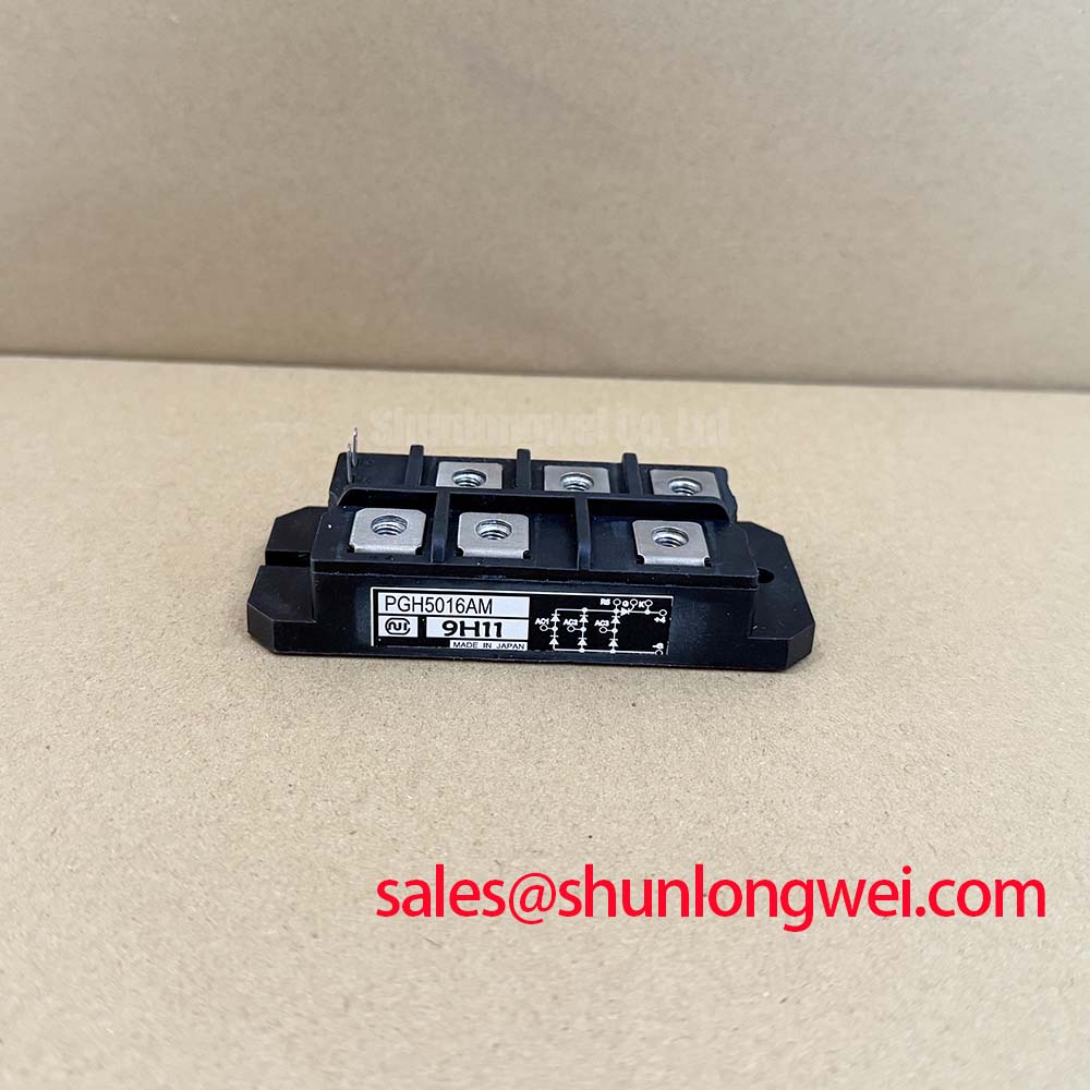
Where the equipment bill of materials permits a cross reference review, PD25016A can be assessed as a separate module option, but voltage class, current rating, terminal arrangement, gate characteristics, mechanical interface, thermal path, and the original circuit requirements must all be verified individually. Matching only the headline voltage rating is not a valid replacement determination.
Transient Dynamics & Electrical Design: Harmonic Current Injection and Line Filter on MCC40 16I06
In a grid tied static var compensator or thyristor switched capacitor bank, confirm the module terminal assignment against the phase switching drawing before energizing the cabinet. The MCC40 16I06 is a 1600V, 40A dual thyristor module, and those official ratings define important device limits, but they do not disclose the firing angle, capacitor stage size, source impedance, line filter specification, or protection settings used in a particular SVC installation.
Thyristor phase control changes the interval during which current is permitted to flow. As the firing angle is moved away from the voltage zero crossing, the resulting current waveform changes with the load, supply impedance, and switching topology. In capacitor switching equipment, transient current and line resonance also depend on capacitor bank condition, reactor configuration, contactor state where used, and the sequencing logic. Engineers should therefore treat harmonic current, displacement power factor, and reactive power behavior as system measurements rather than attributes guaranteed by the module.
Engineering Recommendation: examine the firing command and the line current together during controlled commissioning. A current waveform that differs from a known good phase may indicate a gate drive timing issue, an open protection path, a deteriorated capacitor stage, an incorrect terminal connection, or a supply side condition. Oscilloscope observations should be made with suitable isolation and voltage rating, using a known good signal path as the comparison reference. Do not infer a single root cause from waveform shape alone.
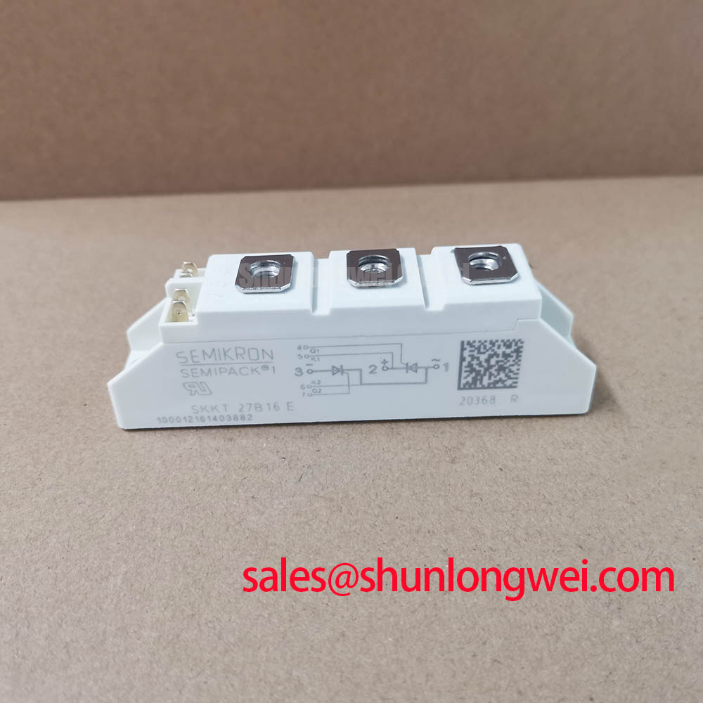
The gate drive supply and its reference path require the same inspection discipline as the power terminals. Verify that firing commands arrive in the intended sequence, that control connections are secure, and that no unintended common reference has been introduced during servicing. A related phase controlled rectifier or supply section may use another power semiconductor module, such as SKKT 106B14E, but each device must be assessed from its own published ratings and connection diagram.
Line filters and snubbers should be evaluated as part of the installed system. Their task may include limiting conducted disturbance, moderating transient behavior, or controlling resonant response, yet their component values and placement must follow the equipment design and measured operating conditions. The module itself does not establish the compliance status of the finished SVC cabinet. For a general product family reference on power semiconductor modules and diodes, consult Shindengen Power Semiconductor Modules and Diodes.
MCC40 16I06 Operational Boundaries: Evaluating Baseplate Thermal Resistance Limits
With the module removed from the heatsink, check the mounting face for residue, raised debris, corrosion, scratches, or evidence that the module was previously clamped unevenly. The official identification available for this device establishes a module package, while a numerical junction to case thermal resistance, allowable junction temperature, mounting torque, terminal torque, and baseplate construction must be confirmed in the specific IXYS datasheet. These details must not be inferred from the 40A current rating.
Design Consideration: a clean, flat mating interface and evenly distributed clamping force help maintain a repeatable thermal path from module to heatsink. Apply the thermal interface material according to the equipment manufacturer procedure and avoid module distortion during fastening. The appropriate torque depends on the hardware, thread engagement, mounting pattern, module documentation, and heatsink material. The system integrator should verify the approved torque rather than applying a generic value as an IXYS requirement.
Thermal performance during repetitive capacitor switching is not described by one steady state number. Junction temperature movement follows the actual pulse pattern, conduction interval, current waveform, heatsink temperature, airflow, thermal interface condition, and load sharing among installed paths. When evaluating an existing cabinet, compare thermal images and measured heatsink temperatures across equivalent phases under the same controlled operating condition. A localized difference can justify further investigation, but it does not independently identify whether the cause is a module, interface material, busbar resistance, gate timing, cooling path, or load imbalance.
Engineering Recommendation: use the published transient thermal impedance information when it is available for the exact device revision, then verify the predicted margin through system level temperature and waveform testing. This approach keeps the assessment tied to actual duty cycle rather than treating continuous current rating as permission for every pulsed load profile. Thermal shock is a packaging reliability concern whose test concepts are discussed in Thermal Shock Testing under MIL STD 202; it does not provide a service life prediction for this module in a specific cabinet.
For broader context on how voltage stress, current stress, gate control, thermal conditions, and layout interact in power conversion assemblies, see the Power Electronics Masterclass. The final suitability decision remains dependent on the original SVC or thyristor switched capacitor system design and verification results.
Benchtop Waveform Tuning: Mitigating Stress Through Gate Firing Pulse Train Timing on MCC40 16I06
At the test bench, first verify gate polarity and terminal mapping from the circuit documentation, then monitor the isolated firing signal before reconnecting the power stage. The MCC40 16I06 contains two thyristor functions in one module package, so confusing the gate or main terminal assignments can prevent intended conduction or create an unintended switching sequence. The correct gate trigger current, gate trigger voltage, latching current, holding current, permissible gate pulse conditions, and gate to cathode limits must be obtained from the relevant official datasheet.
A trigger pulse that is adequate at the controller output may not arrive with the same integrity at the module terminals. Cable routing, connector resistance, reference routing, isolation components, interference, and the state of the control supply can alter the observed signal. A practical bench procedure is to compare the command waveform, the gate terminal waveform, and the associated main current under controlled conditions. If the module does not latch as expected, investigate the complete firing chain and load current conditions before attributing the behavior to one device parameter.
In phase controlled equipment, pulse train firing can be used by the system designer to improve trigger certainty across a selected firing window. The required timing, pulse width, rise behavior, repetition pattern, and gating energy are system determined and must remain within published module limits. Engineers should verify that pulse trains stop or continue according to the original control logic, especially when capacitor switching interlocks, phase synchronization, or fault inhibit functions are active.
Design Consideration: minimize unwanted coupling between gate leads and high current commutation conductors, particularly where rapid current change can disturb the gate reference. Validate the result at the module terminals while observing the actual current response. Do not apply a numerical gate drive prescription from a different thyristor module, even when its voltage class appears similar.
For service work, retain the original gate lead routing and confirm that all control plugs, screening provisions, and mechanical restraints are restored before final waveform checks. The electrical identity to preserve is the documented IXYS 1600V, 40A MCC40 16I06 module installation within its specified circuit, not an assumed set of universal firing values.