


Content last revised on September 22, 2026
Assembly Integrity & Layout Architecture: Preventing Localized Gate Hotspot Burnout for MCD310-16IO1
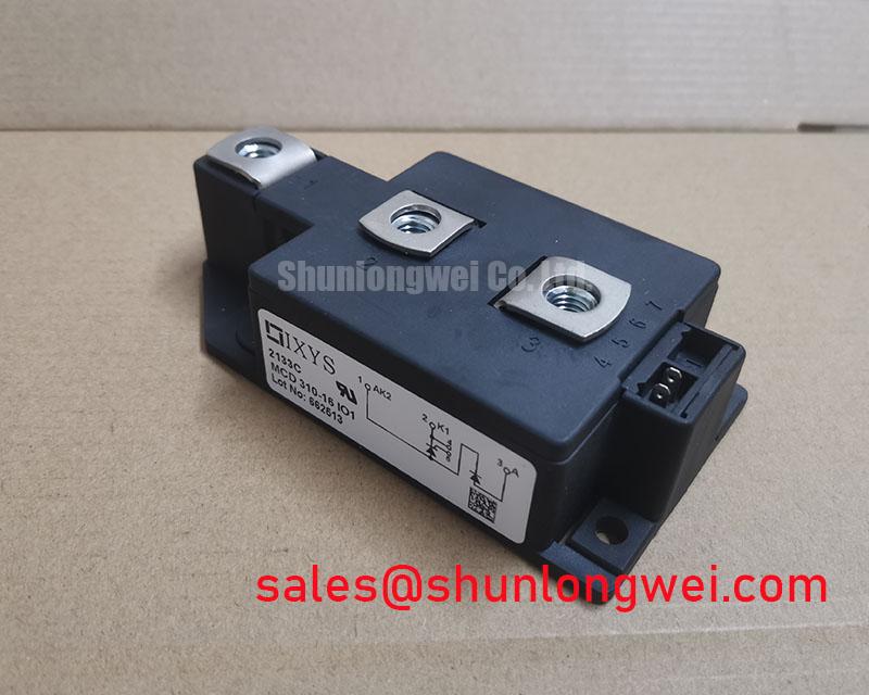
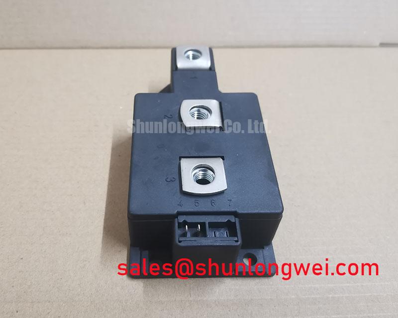
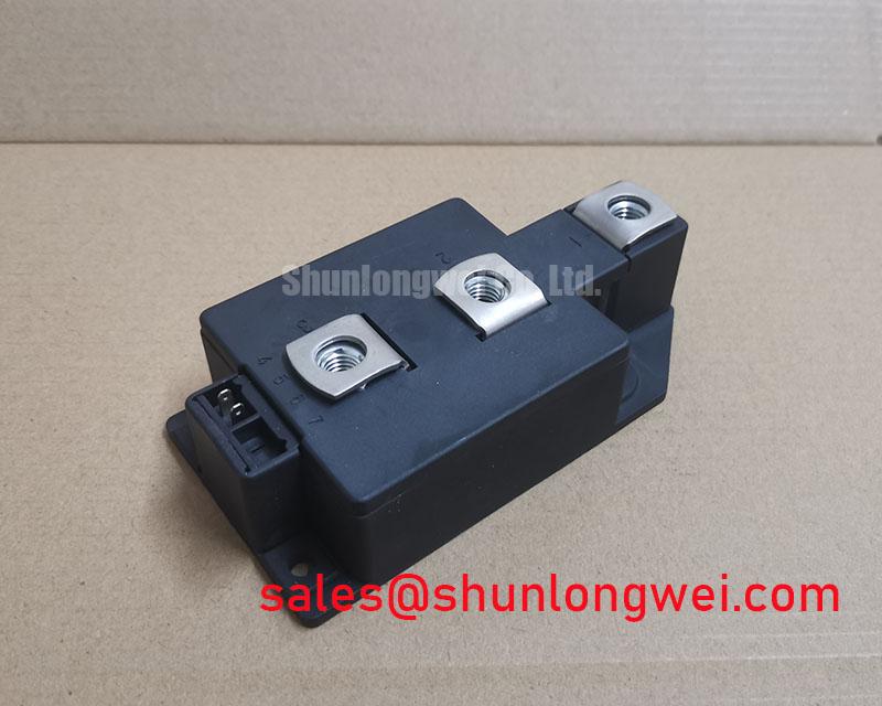
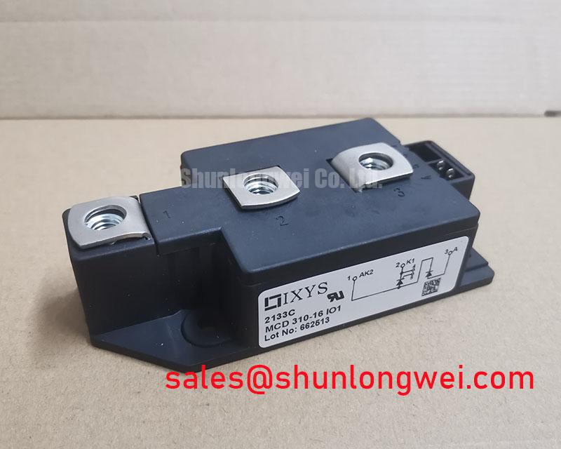
Before installing a replacement, inspect the module body and terminals, verify the marking against the equipment record, and confirm the specified 1600 V and 310 A ratings against the original circuit position. The IXYS MCD310-16IO1 is a Dual Thyristor Module in a TO-240AA package, suitable for evaluation in high-power controlled rectifier and thyristor-switched capacitor assemblies when the complete electrical and thermal conditions are verified by the system engineer.
The first integration task is to establish the exact terminal identity from the original equipment drawing and the applicable IXYS documentation. A dual thyristor module must not be wired from visual assumptions alone. Confirm the anode, cathode, and gate connections for each internal device, then compare cable routing, trigger polarity, and the control board reference point with a known-good assembly.
The published product data supplied for this device identifies a 1600 V voltage rating, a 310 A rated current, and a TO-240AA package. These are official product parameters, but they do not by themselves define the allowable surge current, gate trigger current, gate trigger voltage, holding current, latching current, thermal resistance, or fuse coordination. Those values must be taken from the correct IXYS datasheet revision before a protection or firing circuit is released.
Gate firing quality is especially important when the module is used in a grid-tied static Var compensator or a thyristor-switched capacitor bank. A trigger pulse that reaches one gate path later or with insufficient current can produce uneven conduction between parallel electrical paths, while excessive ringing can cause unwanted triggering. The practical design consideration is to keep the gate loop short, return the gate reference through its intended control path, and separate high-current commutation conductors from low-level trigger wiring.
For phase-controlled operation, the firing controller should be checked across the full intended firing-angle range. The test should confirm that each thyristor receives a repeatable trigger pulse at the intended line phase and that the pulse remains effective under the actual noise environment created by the capacitor bank, reactor, busbar, and switching contactors. The exact IGT and VGT limits are device-specific and should be confirmed from the original electrical documentation rather than inferred from the 310 A rating.
A multi-pulse or pulse-train firing method can be considered when the control architecture and the applicable datasheet permit it. The purpose is to improve trigger reliability during a noisy line transition, not to compensate for an incorrectly wired gate circuit. Any pulse width, repetition rate, gate current, or rise-time target must be selected from the thyristor trigger requirements and validated with an oscilloscope at the module terminals.
Controlled rectifiers and SVC capacitor stages can also create characteristic line-current distortion when the conduction angle is narrow or rapidly changing. Engineers should review the relationship between firing angle, capacitor or reactor impedance, and the upstream network short-circuit strength. Harmonic-current measurements at the point of common coupling should be used to assess the installation against the applicable grid requirements. The module’s voltage and current ratings do not constitute an EMC or harmonic-compliance certification for the complete installation.
| Parameter | Product information | Engineering status |
|---|---|---|
| Manufacturer | IXYS | Product identification |
| Part number | MCD310-16IO1 | Product identification |
| Rated voltage | 1600 V | Official product specification |
| Rated current | 310 A | Official product specification |
| Package | TO-240AA | Official product specification |
| Gate trigger data | Verify from the applicable IXYS datasheet | System integration requirement |
| Fuse I²t coordination | Verify from the applicable IXYS datasheet and fuse manufacturer | Protection study requirement |
When comparing an existing assembly with another dual thyristor device, engineers may review the electrical data and mechanical arrangement of TT570N16 as a separate reference point. It should not be treated as an automatic substitute. Gate characteristics, thermal impedance, terminal geometry, surge capability, and control timing must all be checked before any cross-reference is approved.
Transient Dynamics & Electrical Design: AC Line Surge Immunity and Lightning Transients on MCD310-16IO1
In an SVC or thyristor-switched capacitor installation, the module can be exposed to line transients produced by capacitor energisation, transformer switching, network faults, and external surge events. The 1600 V rating is an important selection parameter, but it is not a complete surge-protection design. The system engineer must compare the actual repetitive and non-repetitive voltage waveform with the device’s blocking and transient ratings from the applicable manufacturer documentation.
Surge protection should be evaluated as a coordinated network rather than as a single MOV placed across the incoming line. The protective arrangement may include upstream fusing, surge arresters or MOVs, an impedance-forming reactor, and an RC snubber located according to the commutation topology. The selected clamping level must remain compatible with the thyristor blocking capability, while leakage current, thermal loading, fault energy, and coordination with upstream protection must also be examined.
For an installation assessed against an impulse-surge standard such as IEC 61000-4-5, the complete equipment assembly is the subject of the immunity test. The MCD310-16IO1 itself should not be described as independently compliant with the system-level standard. The engineer should define the test coupling path, source impedance, protective-device state, and recovery criteria for the finished SVC or capacitor-switching cabinet.
RC snubber selection requires attention to the switching circuit, not only the nominal line voltage. A snubber that is too weak may leave excessive voltage rise across the thyristor; a network with excessive capacitance can increase reactive current, discharge stress, and turn-on demand. The resistor must also be checked for pulse energy and repetitive heating. Exact values should be calculated from the measured commutation waveform and verified against the thyristor’s rated dv/dt and switching conditions.
Field troubleshooting should begin with a de-energized visual inspection of MOV bodies, fuse indicators, snubber resistors, capacitor connections, and terminal insulation. After safe isolation, measure continuity and insulation conditions using procedures appropriate to the cabinet’s voltage class. During controlled energisation, use differential high-voltage probing to observe the voltage across the module and compare it with the control pulse timing. An abnormal waveform may indicate a protection, wiring, commutation, or load-network issue; it should not be assigned to the thyristor without evidence from the surrounding circuit.
Safety Interlock Note: Isolate and verify the absence of stored energy in both the DC or capacitor section and the gate-control supply before touching module terminals or disconnecting the trigger harness.
MCD310-16IO1 Operational Boundaries: Evaluating Saturable Reactor and Snubber Sizing to Protection Limits
A saturable reactor may be used in some high-power switching arrangements to limit the initial current slope and shape the commutation event. Its suitability depends on the capacitor-bank impedance, operating frequency, line voltage, fault level, switching sequence, and the thermal duty of the complete magnetic component. The MCD310-16IO1 rated current of 310 A should therefore be treated as a product boundary for selection review, not as a universal operating current for every SVC topology.
The design consideration is to control the interaction between di/dt, dv/dt, and the available gate-drive margin. Excessive current rise can increase semiconductor stress and busbar-induced voltage overshoot. Excessive circuit inductance can delay current transfer or create an unexpected commutation condition. Engineers should measure the actual current and voltage waveforms at the module terminals during startup, steady switching, abnormal line conditions, and the highest intended capacitor-switching duty.
The RC snubber and saturable-reactor network should be evaluated together. Changing the reactor can alter the voltage transition seen by the snubber, while changing the snubber can affect reactive current and the energy dissipated during each switching event. The correct values are system-determined and should be based on measured waveforms, the applicable thyristor dv/dt and di/dt limits, thermal calculations, and the fuse manufacturer’s clearing characteristics.
Fuse coordination is another important boundary. A semiconductor fuse must be selected using the applicable I²t and peak-current information for the exact module and installation. The fuse’s nominal ampere rating alone is not enough to demonstrate protection. Confirm the prospective fault current, fuse clearing time, let-through energy, repetitive duty, and coordination with the upstream protective device. If the relevant IXYS fuse coordination table is not available for the exact product revision, the protection study should remain open rather than being filled with an assumed value.
In a phase-controlled rectifier or capacitor-switching system, line-current harmonics can increase as the conduction interval becomes more discontinuous. The control system should therefore be checked for firing-angle stability, phase synchronization, and balanced operation between the two internal thyristor paths. Harmonic filters, reactors, and switching schedules belong to the complete installation design. They should be selected from measured network performance and applicable utility requirements, not from the module’s package designation.
During fault investigation, compare the gate waveform, anode-to-cathode voltage, and load current on the same time reference. A missing or delayed trigger may arise from the controller, isolation stage, connector, return path, or gate circuit. A voltage spike may arise from layout inductance, snubber degradation, capacitor-bank resonance, or an upstream surge. The recommended method is to isolate these possibilities through waveform comparison with a known-good phase and by checking the equipment schematic.
For a broader treatment of gate-loop layout, transient measurement, protection coordination, and power-semiconductor reliability principles, engineers can consult the Power Electronics Masterclass. The system designer should still use the MCD310-16IO1-specific documentation for all final ratings and acceptance criteria.
Transient Dynamics & Electrical Design: Mechanical Mounting Torque Sequence and Thermal Considerations on MCD310-16IO1
Mechanical installation directly affects the thermal path from the module base to the heatsink. Before mounting the TO-240AA package, clean both mating surfaces according to the equipment maintenance procedure, inspect the heatsink for burrs or distortion, and confirm that the module sits flat without being forced into alignment by the busbars. The manufacturer’s specified mounting torque and sequence must be obtained from the applicable IXYS mechanical documentation; they should not be inferred from the current rating or package name.
Thermal verification should use the correct IXYS thermal-resistance data for the exact device and mounting condition. The supplied product information confirms the package, voltage, and current ratings, but it does not provide a verified Rth(j-c), baseplate temperature limit, heatsink requirement, or thermal interface thickness. These parameters must be confirmed before calculating junction temperature or approving continuous operation.
Apply the thermal interface material evenly and only in the manner permitted by the module and heatsink instructions. Too little material can leave air gaps, while excessive material can migrate toward insulation surfaces or create an uneven mounting condition. The heatsink should be checked for uniform contact after fastening, and the module should not be used to correct a warped base or misaligned mounting hole.
Busbar installation should follow the mechanical sequence specified for the cabinet. Heavy conductors must be supported independently so that terminal studs do not carry bending force. Keep the high-current path compact and symmetrical where the topology permits, and route the gate wiring away from the strongest commutation field. If the control board uses a separate gate reference or auxiliary return, preserve that separation and confirm continuity before energisation.
The module’s operating temperature must be evaluated from measured heatsink temperature, load profile, switching frequency, ambient conditions, airflow, and enclosure construction. A temperature reading on the heatsink alone does not prove the semiconductor junction is within its specified limit. Thermal measurements should be repeated after the equipment reaches a stable operating condition and after representative overload or switching sequences where those conditions are permitted by the system design.
For maintenance, inspect terminal discoloration, looseness, signs of local heating, cracked insulation, and changes in the snubber or fuse assembly. Compare phase currents and gate waveforms rather than relying on a single temperature measurement. If the module is replaced, record the original wiring arrangement, protection components, heatsink condition, and control timing so that post-replacement behavior can be compared objectively.
The external LVDS architecture reference available from Low-Voltage Differential Signaling Interface Architecture is relevant only to equipment that contains a separate digital display or control interface; it does not define the gate-drive interface of this thyristor module. Any display or controller communication fault should therefore be diagnosed independently from the MCD310-16IO1 power path.