
Content last revised on September 22, 2026
Bench Verification Before Installing T298N12TOF
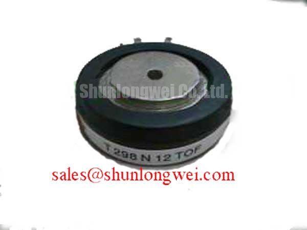
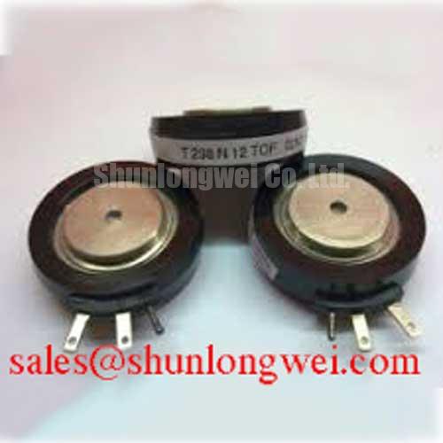
Before installing T298N12TOF, isolate the equipment, confirm the nameplate voltage boundary, and inspect the module body, terminals, and mounting surfaces for transport or installation damage. The available product data identifies this Infineon device as a Thyristor/Diode Module in a PowerBlock Module package with an official rated voltage of 1200.0 V and an official rated current of 298.0 A.
These values identify the principal electrical class of the component, but they do not by themselves establish the allowable current under every ambient temperature, switching condition, overload duration, cooling arrangement, or fuse coordination condition. When replacing a device in a high voltage three phase motor solid state soft starter, the system engineer should compare the original circuit conditions with the manufacturer’s complete electrical and thermal documentation before energizing the assembly.
| Parameter | Value | Classification |
|---|---|---|
| Manufacturer | Infineon | Product identification |
| Part number | T298N12TOF | Product identification |
| Rated voltage | 1200.0 V | Official specification supplied for this product |
| Rated current | 298.0 A | Official specification supplied for this product |
| Package | PowerBlock Module | Official physical classification supplied for this product |
| Product category | Thyristor/Diode Module | Category classification |
A cold resistance measurement across power terminals is not sufficient to prove that a thyristor or diode junction is healthy. It can be used as one part of a controlled inspection routine, provided the circuit is fully disconnected and the measured terminal pair is known. Gate terminals should not be tested with an uncontrolled insulation tester or exposed to a voltage that exceeds the relevant gate rating. The original wiring diagram and the applicable Infineon documentation should be used to identify anode, cathode, gate, and auxiliary connections before any measurement is made.
For procurement and maintenance records, retain the complete part number, package description, electrical class, and the equipment position from which the component was removed. The module should be evaluated as part of the complete commutation and cooling assembly rather than as an isolated current rating.
Snubber and Saturable Reactor Evaluation During Waveform Tuning
In a soft starter, the snubber network and any series saturable reactor influence the voltage and current transitions seen by the thyristor paths. The T298N12TOF product data supplied for this page confirms the 1200.0 V voltage class and 298.0 A current class, but it does not provide a complete snubber value, reactor value, gate drive waveform, fuse I²t coordination table, or mounting torque specification. Those values must be taken from the applicable manufacturer documentation and the original equipment design.
Snubber selection should begin with an oscilloscope measurement of the power terminals during the actual firing and commutation sequence. Designers should examine the peak voltage, ringing frequency, damping behavior, and the timing relationship between the gate command and the power waveform. A measured overshoot should not be attributed to the module alone because busbar inductance, cable length, transformer leakage, snubber placement, probe connection, and the commutation network can all influence the displayed waveform.
A saturable reactor can alter the current rise profile during selected portions of the waveform. Its suitability is system determined. When evaluating one, engineers should verify the current waveform at startup, near rated load, during motor acceleration, and under the most demanding restart condition allowed by the equipment. The measured result should be checked against the semiconductor voltage and current limits, the protective fuse characteristics, and the thermal capability of the complete assembly.
Fuse coordination requires the exact semiconductor protection data rather than a generic fuse recommendation. The engineer should obtain the relevant I²t withstand and coordination information for the specific T298N12TOF revision and compare it with the proposed semiconductor fuse, fault clearing time, prospective current, and installation impedance. A fuse that appears suitable from its continuous current label may still be unsuitable for the transient protection requirement.
Terminal connections deserve the same attention as the snubber values. Keep the snubber loop physically close to the terminals it protects, minimize unnecessary conductor length, and verify that the power connection surfaces are clean and flat. The final arrangement should be validated with a properly rated differential probe and a current measurement method that does not introduce excessive loop area.
💡 Pro Tip: Keep the high current path mechanically symmetrical and confirm the commutation voltage margin with a measured commutation or equivalent transient test before approving the assembly for service.
For a related comparison point during sourcing, engineers may review TD210N12 as a separate product reference, but electrical, mechanical, thermal, and control compatibility must be verified independently rather than assumed from a similar product name or category.
Operational Boundaries in High Voltage Three Phase Soft Starters
A high voltage three phase motor solid state soft starter controls the applied motor voltage and current during acceleration. The motor’s locked rotor current, acceleration time, load torque, line impedance, bypass arrangement, and firing strategy determine the stress imposed on each semiconductor path. The T298N12TOF is identified with a 1200.0 V rated voltage and 298.0 A rated current, yet those figures should not be converted directly into a guaranteed motor horsepower, starting current, or overload duration without the missing thermal and dynamic conditions.
During commissioning, record the line to line voltage, phase current, firing angle or control command, motor acceleration profile, and semiconductor temperature response. The aim is to confirm that all three phases share the expected electrical duty. Unequal phase current may indicate a control timing issue, a connection problem, a measurement error, an upstream supply imbalance, or a device path that requires further testing. It should not be assigned to one cause without comparison against a known good waveform.
Mechanical torque reduction is also a system level result. A soft starter may reduce the abrupt application of motor torque, but the actual result depends on the driven load, motor design, ramp profile, current limit, bypass transition, and control loop response. Engineers should tune the control system from measured motor current and shaft behavior rather than apply a universal current multiplier or ramp value.
When the motor cable is long, the cable impedance and installation geometry can influence the voltage waveform at the motor and at the starter terminals. Reflections, grounding arrangement, shield termination, and switching rate should be considered during testing. Any apparent high voltage peak should be measured at the relevant physical location because a reading at the controller may not represent the motor terminal condition.
Thermal verification should include the complete heat transfer path. Confirm that the heat sink, interface material, clamping method, airflow or liquid cooling arrangement, and temperature sensor location match the equipment design. The package description alone does not specify a permitted clamping force or a universal mounting torque. Those mechanical values must come from the applicable device documentation and the mechanical assembly drawing.
For replacement work, compare the terminal arrangement and physical envelope before removing the original device. A replacement with the same broad voltage and current class can still be unsuitable if its terminal geometry, gate connection, thermal interface, or triggering requirements differ. The system integrator should verify every connection against the original schematic and the appropriate Infineon technical documents.
The broader topics of gate drive layout, thermal management, protection coordination, and circuit topology are discussed in this IGBT Design and Integration reference. It should be treated as an engineering resource, not as a substitute for the specific T298N12TOF data required for final approval.
Gate Trigger Dynamics and Protection of the Firing Circuit
The gate circuit must deliver a controlled trigger signal to the correct thyristor terminal while remaining electrically coordinated with the phase control system. The supplied product information does not specify gate trigger current, gate trigger voltage, pulse rise time, latching current, holding current, allowable repetitive gate power, or a mandatory multi pulse firing pattern for T298N12TOF. These parameters should be obtained from the applicable Infineon datasheet or technical documentation before a driver is designed or repaired.
During troubleshooting, inspect the gate pulse at the module terminals rather than relying only on the controller output. A pulse that looks correct at the control board can be distorted by isolation components, transformer leakage, wiring impedance, connector resistance, or an incorrect return path. The gate waveform should be compared across all relevant phases and under the operating conditions where the fault appears.
Gate loop inductance can produce ringing and delay the transfer of trigger energy. A practical design consideration is to keep the gate and return conductors closely coupled, route them away from high current commutation loops, and avoid sharing the gate return with noisy control currents. The final damping arrangement is system determined and should be verified with a differential measurement method suitable for the gate circuit.
A repeated firing sequence can be useful when the control architecture and device documentation support it, but a multi pulse strategy must not be introduced solely to compensate for an unknown gate connection or insufficient driver capability. The engineer should confirm the required trigger pulse width, current, repetition behavior, and isolation performance from the component documentation. The gate circuit should also be checked during supply variation and at the expected equipment temperature range.
Protection review should include the driver supply, isolation barrier, gate resistor arrangement, transient suppression, and the physical separation between power and control wiring. An apparent failure to trigger may result from control timing, insufficient pulse energy, an open connection, excessive noise, or a power path issue. Use continuity checks, controlled low energy tests, and waveform comparison to narrow the investigation without assigning a single cause prematurely.
Infineon’s EasyPACK™ power semiconductor reference provides useful background on power module integration, but it should not be interpreted as a specification for the gate behavior of T298N12TOF.
Reverse Recovery and Commutation Stress Assessment
Where the assembly uses diode paths for commutation or freewheeling, reverse recovery behavior affects current redistribution, voltage overshoot, switching loss, and conducted or radiated disturbance. The product information supplied here identifies T298N12TOF as a thyristor/diode module, but it does not state reverse recovery charge, reverse recovery time, peak reverse recovery current, softness factor, junction temperature limits, or a temperature coefficient. Those values must be confirmed from the applicable manufacturer data before a loss or EMI calculation is made.
Measure the commutation waveform at the semiconductor terminals and at the associated bus structure. The test should capture forward current, reverse current, voltage recovery, ringing, and the effect of snubber components. Probe grounding and sensor bandwidth should be controlled because an unnecessarily large measurement loop can create a misleading high frequency waveform.
Reverse recovery stress is influenced by the line inductance, transformer characteristics, motor cable, firing angle, load current, temperature, and the interaction of other phases. A single waveform at light load cannot establish the behavior of the complete soft starter. Engineers should test the operating points that represent startup, steady operation, bypass transfer, controlled stop, and abnormal but permitted supply conditions.
EMI compliance belongs to the complete equipment. The T298N12TOF module itself should not be described as independently certified to CISPR, EN 55011, or another system level EMC requirement. The enclosure, cable routing, grounding, filtering, snubber layout, and switching control must be assessed together by the equipment manufacturer or system integrator.
High altitude, cosmic ray effects, single event burnout, FIT rate, service life, insulation reliability, and safety certification also require documented device or system sources. No specific failure rate, lifetime claim, altitude derating value, or certification status should be inferred from the 1200.0 V and 298.0 A ratings alone. For field repair, record the actual operating voltage, current, temperature, fault waveform, protection response, and mechanical condition so that the replacement decision remains traceable to measured equipment conditions.
After the electrical and mechanical checks are complete, verify phase balance, gate timing, thermal response, and protective trip behavior under controlled commissioning conditions. The final acceptance criteria should come from the soft starter manufacturer, the applicable Infineon documentation, and the responsible system engineer.