

Content last revised on October 9, 2026
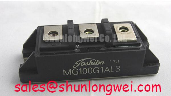
MG100G1AL3 Thermal-Electrical Optimization: High-Frequency Common-Mode Bearing Current Practical Tuning
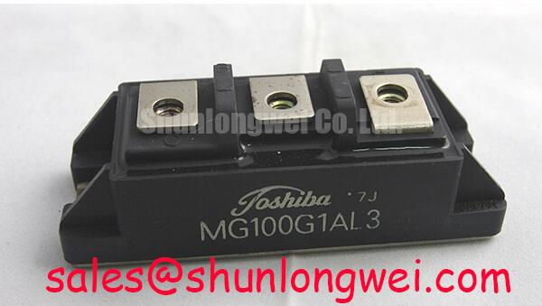
| Product model | MG100G1AL3 |
|---|---|
| Manufacturer | Toshiba |
| Product category | IGBT Module |
| Rated voltage | 600.0 V — Official Specification |
| Rated current | 100.0 A — Official Specification |
| Package | Toshiba Module |
| Integration reference | Consult Datasheet for terminal assignments, rating conditions, switching characteristics, thermal limits, and mounting requirements. |
Measure the switching waveform at the module terminals separately from the waveform at the remote load before attributing a voltage spike to the MG100G1AL3. As a Design Consideration, these measurement locations distinguish local commutation overshoot from cable reflection. Use appropriately rated differential probes with short connections, and record the DC-link voltage, load condition, cable arrangement, and switching state alongside each capture.
The module’s 600.0 V voltage rating defines a device boundary, not a target operating bus voltage. An integration assessment should account for the actual voltage across the switching device during turn-off, including disturbances associated with the power loop. The 100.0 A current rating likewise needs its specified thermal conditions when assessing sustained operation. Neither value alone establishes an acceptable switching frequency or heatsink requirement.
For a motor-drive installation, long leads behave as transmission lines when the switching edge is sufficiently fast relative to cable propagation time. Design Consideration: an idealized high-impedance load termination can produce a reflected terminal step approaching twice the incident voltage step. This is not a guaranteed MG100G1AL3 waveform, and the motor-terminal voltage should not be equated directly with the voltage across the module. Cable losses, termination impedance, edge shape, and repeated reflections affect the measured result.
Compare traces at the inverter output and motor terminals using a consistent probe setup. A delayed excursion at the remote termination supports investigating cable reflections; ringing concentrated at the switching device calls for closer examination of the local commutation loop. Probe placement can itself introduce misleading oscillation, so repeat suspicious measurements with reduced measurement-loop area before modifying the circuit.
Output dv/dt filters and chokes should be evaluated against the measured edge behavior, cable characteristics, load current, and permitted voltage drop. Their inductance, damping, thermal capacity, and resonance behavior are system decisions. Differential-mode filtering addresses phase-to-phase stress, while common-mode mitigation concerns current returning through capacitance and grounding paths. Treating these as interchangeable functions can leave the original disturbance unresolved.
Where a connected motor exhibits bearing-current concerns, assess the common-mode voltage and its return paths through the cable shield, frame, protective bonding, and machine structure. Design Consideration: high-frequency displacement current depends on both voltage transition rate and distributed capacitance. A lower phase-to-phase overshoot does not by itself demonstrate reduced bearing current. Compare the relevant current and voltage measurements before and after a proposed filter change.
At the module, reduce the enclosed area of the DC-link commutation path and place the effective local decoupling connection close to the switching loop. Overlapping supply and return conductors can reduce loop inductance when their insulation and mechanical construction suit the system. Preserve required clearances around terminals and mounting hardware; derive those clearances from the equipment’s applicable insulation-coordination requirements rather than from the package name.
Thermal assessment should use the actual switching waveform, conduction duty, cooling conditions, and manufacturer loss data. Increasing gate damping to soften an edge can change switching loss, while adding an output filter introduces its own heating. Record case-temperature behavior after the operating point stabilizes and evaluate it through the documented thermal model. A cool heatsink surface does not independently establish a safe junction temperature.
The discussion of Power Inverter Topologies and Pulse-Width Modulation (PWM) provides background on bridge switching and output modulation. For this module, the useful comparison is between the host circuit’s switching sequence and the measured current paths: identify which device commutates, where recovery current flows, and which loop produces the observed disturbance.
Field Diagnostics & Commissioning: Dynamic Braking Chopper Operation in MG100G1AL3 Topologies
Trace the braking branch from the DC link to its switching device and resistor before assessing whether the MG100G1AL3 is compatible with that position. Identify the control signal, current path, protective elements, and resistor connection from the equipment schematic. An external braking branch must be evaluated as a complete circuit; the module’s voltage and current ratings do not establish a built-in braking function.
Design Consideration: during regenerative deceleration, energy returned by the load can raise the DC-link voltage when the supply cannot absorb it. A braking chopper diverts energy into a resistor under controller supervision. Resistor selection therefore depends on returned energy, peak braking power, repetition rate, cooling, and the resistor manufacturer’s pulse limits. Its resistance also determines the switch current at the operating bus voltage.
Commissioning should correlate DC-link voltage with the chopper command and measured braking current. If the bus rises unexpectedly, investigate whether the controller requests braking, whether the gate waveform reaches the device, and whether the resistor branch carries current. An open connection, incorrect control behavior, resistor damage, or a switching fault can produce overlapping symptoms; the waveform sequence helps separate these possibilities without assigning a single cause prematurely.
Review the braking switch’s turn-off event independently of the main inverter output. The resistor wiring and its return conductor form a switching loop that can generate local overshoot. Keep the outgoing and returning paths closely coupled where the mechanical design permits, and assess any suppression network against measured energy and repetitive heating. A physically remote resistor requires attention to its connecting conductors, not just its resistance value.
Parallel-device arrangements introduce another compatibility question. A positive temperature coefficient of collector-emitter saturation voltage can assist static sharing in an appropriate operating region, but it must be established from the relevant device characteristics rather than assumed for every IGBT. Dynamic sharing also depends on gate timing, driver impedance, device variation, and commutation-path inductance. Static current balance cannot validate switching balance.
For a parallel implementation under evaluation, compare the current in each branch during conduction and switching, together with the corresponding gate-emitter waveforms. Symmetrical busbars and comparable driver paths help reduce imposed imbalance, but terminal geometry and cooling contact also matter. Look for repeatable differences under matched conditions before changing gate components or concluding that a module is responsible.
Practical design tip: Keep parallel commutation paths geometrically balanced, then use controlled double-pulse testing to check current sharing and turn-off voltage margins before full-power commissioning.
A procurement comparison with MG50J6ES40 should begin with circuit configuration, voltage class, current-rating conditions, terminal layout, and mechanical fit, followed by switching and thermal characteristics. It is a separate Toshiba model to assess, not an established drop-in replacement. Matching a brand or a portion of the model designation does not demonstrate compatibility with the existing driver or braking branch.
For adjacent power-stage planning, MG75Q1ZS50 can be included in a separate component review where the schematic identifies an auxiliary switching position. Its suitability for that position must follow its own specifications. Do not assign it a front-end rectifier role simply because it appears in the same power-module procurement comparison.
Potential application assessments include an industrial inverter welder or medium-frequency induction heating supply, subject to the host circuit’s switching frequency, load behavior, cooling, and protection requirements. These circuits are not automatically equivalent to regenerative motor drives. The background on Solar Inverter Topologies and Grid-Tied Systems illustrates why energy-flow direction and DC-link control depend on topology; it does not establish a solar application approval for this module.
MG100G1AL3 Circuit Protection & Reliability: Diagnosing Gate-Emitter Insulation Issues
Disconnect the module from external power and driver paths, verify that stored energy has been discharged, and identify the terminals from the connection diagram before using a multimeter. Engineering Recommendation: cold screening should distinguish the module’s behavior from parallel components on the board. Snubbers, resistor networks, and connected driver circuitry can alter readings and obscure the path actually being tested.
In diode-check mode, examine the main-terminal paths in both polarities while controlling the gate state according to the service procedure. Where the module connection diagram identifies an antiparallel diode, compare its indicated conduction direction with that diagram. Record the meter, polarity, and test conditions. A repeatable discrepancy warrants investigation, but a universal forward-voltage acceptance band should not be imposed without the relevant test specification.
Gate-emitter screening can identify an obvious low-resistance path, but an ordinary digital multimeter does not qualify gate dielectric integrity or measure switching threshold reliably. The reading is influenced by gate capacitance, meter behavior, and connected protection components. Compare suspect results with a known-good unit under the same setup, and reserve acceptance decisions for the manufacturer’s specified electrical tests and suitable test equipment.
Examine the gate drive at the module terminals during controlled energization. Design Consideration: collector voltage transitions can couple current into the gate through collector-gate capacitance, producing unwanted gate excursions if the return path or driver impedance is unsuitable. Evaluate the off-state waveform alongside the complementary switch transition, separating genuine gate movement from probe-induced artifacts.
Keep the gate command and its return closely coupled and separate them from high-current commutation routing. If the documented terminal arrangement includes a dedicated auxiliary emitter connection, use it as intended for the driver reference rather than sharing the main power-return path. This is a conditional integration principle, not a claim that MG100G1AL3 has a Kelvin-emitter terminal.
Gate resistance, turn-off control, and any Miller-clamp implementation should be assessed as a coordinated driver design. Damping can reduce oscillation, but excessive slowing changes switching dissipation and commutation behavior. Validate the resulting waveforms across the intended operating conditions rather than adopting a resistor value from another module installation.
Check the host protection sequence, including fault detection, driver response, and restart behavior, against the device’s documented limits. The Power Electronics Masterclass provides broader selection and reliability context. For the MG100G1AL3 product assessment, retain the actionable test record: isolated-terminal screening results, gate waveforms, switching voltage excursions, thermal observations, and the equipment conditions under which each measurement was obtained.