



Content last revised on October 29, 2026
MG200J6ES61 Ratings and Pre-Test Checks
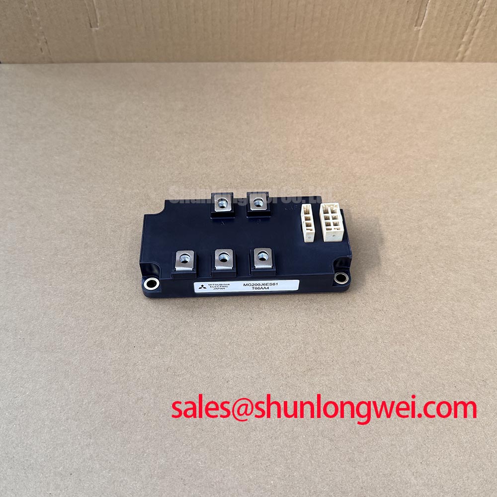
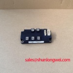
Before connecting the device to a test fixture, confirm the Toshiba marking, isolate the module from all power sources, and verify the intended collector, emitter, and gate connections against the original equipment documentation. The supplied product data identifies the MG200J6ES61 as a Toshiba IGBT Module with a specified voltage rating of 600.0 V and a specified current rating of 200.0 A. Its listed package is Toshiba Module. The current-rating conditions must be checked in the applicable Toshiba documentation; the listed value alone does not establish an allowable continuous operating current.
| Manufacturer | Toshiba |
| Model | MG200J6ES61 |
| Product category | IGBT Module |
| Rated voltage | 600.0 V, supplied product data |
| Rated current | 200.0 A, supplied product data; rating conditions require confirmation |
| Package | Toshiba Module, supplied product data |
The voltage and current figures define important nameplate boundaries, but they do not by themselves establish allowable switching frequency, short-circuit withstand time, thermal impedance, gate-drive voltage, insulation rating, or safe operating area under every operating condition. Those values must be confirmed from the applicable Toshiba documentation and the original equipment design before replacement or commissioning.
Thermal Feedback and VCE(sat) Positive Temperature Coefficient Equalization
For a commercial string inverter or micro-grid energy storage converter, begin the current-sharing assessment with the complete thermal path rather than the module label alone. Measure heatsink contact, interface condition, cooling airflow, and the temperature distribution across parallel switching positions. The MG200J6ES61 carries a listed 600.0 V voltage rating and 200.0 A current rating, but those values are not a substitute for a thermal model using the actual switching waveform, duty cycle, ambient temperature, and cooling arrangement.
When IGBT devices operate in parallel, a positive temperature coefficient of on-state voltage can support steadier static current sharing because a warmer device may develop a higher conduction voltage and therefore attract less current. This is a Design Consideration, not a guaranteed electrical characteristic for this specific model unless confirmed by the manufacturer’s electrical tables. Static sharing and dynamic sharing are separate checks. During turn-on and turn-off, unequal gate-loop inductance, different emitter return paths, and unequal stray inductance can cause one device to switch earlier or later even when the modules have similar markings.
Use physically symmetrical gate-drive routing wherever the circuit places devices in parallel. Keep the forward gate path and the gate-emitter return path similar in length and impedance, and avoid routing a high-current commutation trace beside one gate loop while the other gate loop follows a different path. Clearance should be evaluated against the converter’s working voltage, transient overshoot, pollution environment, and applicable insulation rules; the module’s 600.0 V rating does not define the required board clearance.
During commissioning, compare collector-emitter voltage, gate-emitter voltage, and current sharing at the same operating point. A thermal camera can help locate an imbalance, but it should be correlated with oscilloscope measurements because a brief switching mismatch may not appear as a large steady-state temperature difference. If one position runs hotter, inspect mounting flatness, interface material, current-bar geometry, gate resistance matching, and the return-current path before assuming the semiconductor itself is the only cause.
For a neutral cross-reference exercise, engineers may also review the related Toshiba listing MG20G6EL1. A related part should not be treated as a drop-in replacement until its voltage, current, terminal arrangement, gate requirements, thermal data, mechanical dimensions, and switching characteristics have been matched to the original design.
Desaturation Detection and Two-Stage Soft Turn-Off Short-Circuit Protection
In an inverter bridge, desaturation protection observes whether the conducting IGBT develops an unexpectedly high collector-emitter voltage after the gate command has enabled conduction. This protection signal is not automatically identical to the normal data-sheet parameter VCE(sat). The sensing threshold, blanking interval, diode network, noise filter, and driver response are system-level design variables and must be selected from verified switching waveforms and the gate-driver manufacturer’s application data.
For a Type I or Type II short-circuit protection strategy, the control designer may establish a sub-10 µs response target as an Engineering Recommendation when the measured short-circuit withstand capability and SCSOA information support that approach. The supplied product data does not confirm a sub-10 µs limit or a short-circuit withstand time for the MG200J6ES61. Engineers should obtain the relevant Toshiba switching and short-circuit curves before treating any protection interval as valid.
A two-stage soft turn-off sequence can reduce the abrupt current interruption that otherwise increases stray-inductance voltage. The first stage limits gate discharge or controls the initial current fall, while the second stage completes turn-off after the driver has identified the fault condition. The actual timing and gate-current profile must be verified with a differential high-voltage probe and a properly rated current measurement method. A protection circuit that reacts quickly but has excessive loop inductance can still create a damaging collector-emitter overshoot.
Phase-angle conduction control and line-frequency ripple smoothing should be reviewed together in energy-storage and string-inverter systems where those control methods apply. A control loop that permits a large low-frequency current envelope can alter junction temperature and change the apparent desaturation waveform. A desaturation circuit should therefore be tested at startup, steady load, regenerative operation where applicable, and controlled fault conditions. Do not use a single bench waveform as proof of protection across the full DC-link operating range.
RC snubbers may be evaluated to reduce ringing caused by commutation inductance and device capacitance. Their values are not specified in the supplied MG200J6ES61 data and must be determined from measured ringing frequency, voltage overshoot, dissipation, and the complete bridge layout. The interaction between Ciss, Coss, Crss, gate-driver impedance, and power-loop inductance is explained in this reference on parasitic capacitance in power MOSFETs and IGBTs. Treat that material as general semiconductor background rather than model-specific Toshiba data.
Bench Tip: Keep the module protected against ESD, discharge the DC link fully, and perform cold-state diode-mode checks only as a comparative screen; a multimeter reading cannot replace a rated high-voltage insulation test or a controlled dynamic switching test.
Differential Gate-Emitter Loop Routing to Suppress Ground-Bounce Noise
IGBT terminology normally uses gate and emitter rather than gate and source. Before probing the MG200J6ES61, identify the actual terminal names from the package drawing and the equipment schematic. Do not assume that a module provides an auxiliary Kelvin emitter terminal simply because another IGBT package uses one. The supplied product information confirms the Toshiba Module package category but does not provide a detailed terminal map in the stated data.
The gate-drive loop should be treated as a differential circuit: the driver output travels to the gate, and the return follows the intended emitter reference back to the same driver. A high-current emitter trace shared with the gate-return path produces a voltage disturbance when its current changes rapidly. That disturbance can alter the actual gate-emitter voltage, causing delayed turn-off, unwanted turn-on, or apparent oscillation. Separating the power emitter path from any verified auxiliary emitter return is a Design Consideration that must follow the manufacturer’s terminal configuration.
Place the driver close to the module when the mechanical design permits, keep the gate and return conductors tightly coupled, and avoid routing the gate signal across the switching node. The required clearance from the collector or phase node depends on working voltage, transient voltage, insulation system, pollution level, and certification requirements. It should be confirmed by the system engineer rather than inferred from the 600.0 V device rating.
When a converter shows intermittent gate ringing, compare the gate-emitter waveform directly at the module terminals rather than at the driver output. Check the probe connection, driver supply decoupling, gate resistor location, connector contact resistance, and mechanical vibration at the busbar. A mismatch that appears only under load may be caused by common-emitter inductance, probe error, or a changing commutation path. The IGBT physics and operation reference provides general context for the relationship between gate control, carrier conduction, and switching behavior.
Incoming inspection should document the terminal orientation, package condition, and cold electrical comparison against an approved reference unit. It should not apply a gate voltage or collector voltage outside the manufacturer’s stated test conditions. For field repair, record the original busbar arrangement before removal, because reversing a laminated connection or extending one gate return can change the switching waveform even when the replacement part has the same model marking.
High dv/dt Cross-Conduction Shoot-Through Mitigation with Dedicated Miller Clamps
High dv/dt at one bridge position can couple through the reverse-transfer capacitance of the opposing IGBT and raise its gate-emitter voltage. If that induced voltage exceeds the effective turn-on threshold under the actual temperature and driver conditions, cross-conduction becomes a system risk. This behavior depends on the module’s capacitances, gate impedance, commutation loop, driver architecture, and bus voltage. The supplied product data does not establish a specific dv/dt immunity value for the MG200J6ES61.
A dedicated active Miller clamp is a possible Design Consideration when the driver can detect that the gate has fallen below its clamp threshold and provide a low-impedance discharge path during the opposing device’s turn-on. The clamp layout should be short, referenced to the correct emitter point, and isolated from the high-current return path as required by the driver design. The appropriate clamp current and activation threshold must be confirmed through double-pulse testing and gate-emitter measurements at the module terminals.
Negative gate bias may also be evaluated by the system designer, with a range such as −5 V to −15 V treated only as a general application consideration, not as an official MG200J6ES61 requirement. The allowable gate-emitter range, driver supply arrangement, turn-off behavior, and insulation coordination must come from the applicable Toshiba and gate-driver documentation. Excessive negative bias can create its own reliability and driver-stress concerns, so it should not be selected by habit.
During a double-pulse test, monitor the gate-emitter voltages of both the commanded-off IGBT and the opposing IGBT while measuring the switching-node voltage. A gate waveform that looks clean at the driver may contain a short positive excursion at the module caused by common-emitter inductance or probe placement. Compare the result with the DC-link voltage, load current, junction-temperature condition, and busbar configuration used in the final converter. The objective is to verify peak voltage and gate margins against measured system transients, not to assume that the nameplate rating guarantees immunity to every switching event.
For broader troubleshooting coverage covering gate-drive faults, thermal interfaces, switching transients, and field measurement methods, engineers can consult the Field Engineer’s Handbook. It should be used alongside the applicable Toshiba documentation and the converter manufacturer’s service procedure. The MG200J6ES61 remains identified by the supplied product data as a Toshiba IGBT Module rated at 600.0 V and 200.0 A; final suitability depends on verified electrical, thermal, mechanical, and protection conditions in the target equipment.