Content last revised on September 12, 2026
MG300M1FK1 Replacement Checks
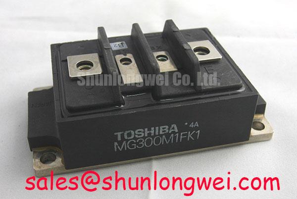
Before fitting the replacement, isolate the equipment, inspect the module body and terminals, and verify the nameplate limits against the circuit documentation: MG300M1FK1 is a Toshiba IGBT Module specified at 600.0 V and 300.0 A. A cold resistance comparison between the power terminals and a known good unit can help identify an obvious abnormality, but it is not a substitute for a controlled semiconductor test or the manufacturer’s application data.
The available factory information identifies the device as a Toshiba Module with a rated voltage of 600.0 V and a rated current of 300.0 A. Gate drive voltage, collector-emitter saturation voltage, short-circuit withstand time, thermal resistance, internal circuit topology, terminal arrangement, dimensions, and mounting specifications should be confirmed from the original Toshiba documentation or the equipment service manual before installation. These values should not be inferred from the current rating alone.
For repair engineers and procurement teams, the key task is to match the electrical boundary, mechanical interface, gate-drive arrangement, cooling method, and switching duty of the existing assembly. The part may be evaluated in industrial inverter welders and medium-frequency induction heating power supplies, subject to confirmation of the original circuit topology and operating profile.
MG300M1FK1 Circuit Protection & Reliability: Calibrating Thermal Cycling Margins in Braking Circuits
When this Toshiba module is used in an inverter power stage, braking performance depends on the complete DC-link system rather than on the IGBT rating in isolation. During motor deceleration, stored mechanical energy can return to the DC link. The braking circuit must then coordinate the braking switch, ballast resistor, DC-link capacitor, current sensing, and protective control so that the energy is absorbed without exceeding the electrical or thermal limits documented for the installed device.
Design Consideration: Select the braking resistor and duty cycle from the actual deceleration energy, repetition rate, DC-link voltage, enclosure temperature, and cooling capability. A resistor that survives one event may still create unacceptable thermal cycling when braking repeats frequently. Designers should calculate pulse energy and average dissipation from the machine profile, then validate resistor temperature, module case temperature, and DC-link voltage during the most demanding operating sequence.
For an industrial inverter welder, inspect the braking branch for loose power connections, discoloration, cracked resistor bodies, and signs of repetitive thermal stress. For a medium-frequency induction heating supply, review the relationship between switching frequency, bus ripple, and cooling airflow before attributing a fault to the module. A thermal camera or correctly positioned thermocouple can reveal an uneven temperature pattern, while an oscilloscope can confirm whether the DC-link rises abnormally during commanded deceleration.
Physical installation also matters. Keep high-current conductors separated from control wiring, provide clearance consistent with the equipment insulation design, and prevent resistor heat from directly warming the module housing or gate-drive board. The heatsink contact surface should be clean and flat, with the approved thermal interface material applied according to the equipment manufacturer’s procedure. Maintenance teams should record the condition of the fan path, heatsink fins, and air filters during scheduled service rather than waiting for an over-temperature trip.
When evaluating an alternative Toshiba module, compare terminal geometry, gate-drive requirements, internal connections, and thermal interface dimensions instead of relying on a similar current label. The MG150Q1JS40 can be reviewed as a separate Toshiba module for comparison, but suitability remains system-dependent and requires confirmation against the original schematic and mechanical arrangement.
Maintenance Note: Monitor operating temperature at the module case and check the cooling path during preventive maintenance, especially after repeated braking or high-duty welding cycles.
Preventing Spurious Faults: Turn-Off di/dt Induced Vpeak Clamping and Guidelines for MG300M1FK1
Turn-off behavior should be checked at the actual module terminals, not only at the gate-driver output. Stray inductance in the commutation loop converts rapid current change into voltage overshoot, so the measured collector-emitter peak can exceed the steady DC-link value. In engineering terms, the transient is related to the DC-link voltage, loop inductance, and current fall rate. This relationship is useful for diagnosis, but the allowable peak must be established from the official device data and the system’s measured switching waveform.
Engineering Recommendation: Minimize the commutation loop area with a short, symmetrical laminated bus structure and place any approved snubber close to the switching path. The capacitance, damping resistance, voltage rating, pulse current, and physical placement must be selected from measured ringing and switching loss. Do not assign a universal inductance target or snubber value to this model without validating the complete power layout.
During commissioning, use a suitably rated differential voltage probe and a current probe with adequate bandwidth. Compare turn-on and turn-off waveforms at light load and at the intended operating load, then inspect the gate signal for ringing, plateau disturbance, or unexpected delay. A nuisance over-voltage or gate fault may also arise from probe grounding, control-reference movement, driver supply disturbance, or an incorrectly routed emitter return, so the signal path should be checked against a known-good channel.
Desaturation protection is a system-level function. The driver designer must verify the sensing method, blanking interval, propagation delay, fault response, and soft turn-off behavior against the selected gate driver and the switching conditions. A two-stage soft turn-off sequence can reduce electrical stress in some protection architectures, but its timing and gate-current profile must be established by the control designer and verified on the bench. The available factory data supplied for MG300M1FK1 does not establish a universal short-circuit detection time or safe operating area for every converter.
Industry technical references can help engineers understand the switching behavior of IGBT technologies. The ROHM Field Stop Trench IGBTs and Intelligent Modules resource and the STMicroelectronics STPOWER IGBTs and Power Transistors resource provide general semiconductor application context. They should not be treated as specifications for this Toshiba module.
Transient Dynamics & Electrical Design: Dynamic Power Loss Dissipation and Thermal Modeling for MG300M1FK1
A replacement decision should include transient thermal behavior, not just the continuous 300.0 A rating. In inverter welders and induction heating supplies, conduction and switching losses vary with current, duty ratio, bus voltage, frequency, gate resistance, junction temperature, and load waveform. The module case may appear acceptable while the junction experiences a much larger short-duration temperature excursion during overload or repetitive pulsing.
Design Consideration: Use the official transient thermal impedance data for the exact device and model the heat path from junction to case, interface material, heatsink, and cooling environment. A multi-resistance, multi-capacitance thermal model can estimate the junction response to pulse loading, but the result remains an engineering calculation until verified with measured case temperature and validated loss data. The system engineer should test the worst credible pulse sequence rather than relying on a single steady-state thermal reading.
For field troubleshooting, first document the operating waveform, switching frequency, load current, DC-link voltage, ambient temperature, and duration of the fault. Then inspect the thermal interface for pump-out, dry areas, contamination, or uneven pressure. Check that the heatsink is not distorted and that the airflow path has not been restricted by dust or a displaced duct. If a thermal trip occurs only after repeated cycles, compare the timing of the trip with resistor heating, fan operation, bus ripple, and gate-drive temperature.
Battery charge and discharge converters can also produce repeated bidirectional thermal loading. If the system uses this module in such a topology, designers should evaluate both current directions, regenerative transitions, dead-time behavior, and the thermal effect of alternating power flow. Any claimed lifetime improvement must be supported by an appropriate qualification report or field-data source; it should not be estimated from the nominal current rating alone.
Keep the thermal design traceable. Record the interface material type, heatsink condition, fan status, and measured case temperature after service. If the module is replaced, compare the new waveform and temperature profile with the previous installation under the same controlled load. This approach helps separate a module-related issue from airflow degradation, excessive switching loss, resistor heating, or a control-loop problem.
Transient Dynamics & Electrical Design: Auxiliary Emitter Return Trace Separation on MG300M1FK1
The gate-drive return path should be treated as a sensitive measurement reference, while the main emitter path carries high and rapidly changing current. If these paths share an uncontrolled section of copper, the voltage developed by common impedance can appear at the gate-driver reference and disturb the intended gate-emitter command. The resulting waveform may include ringing, delayed turn-off, uneven current sharing, or intermittent protection trips.
Engineering Recommendation: Route the auxiliary emitter return separately from the main high-current emitter conductor for as much of the external circuit as the module interface permits. Keep the driver loop compact, avoid parallel routing with the collector bus, and use a controlled reference point defined by the original schematic. The required geometry is determined by switching speed, current, board construction, and measured common-mode noise, so it must be verified with differential measurements at the module terminals.
During a fault investigation, compare the gate-emitter waveform directly at the module with the signal measured at the driver output. A difference between these locations may indicate return-path coupling, driver supply movement, probe error, or an unsuitable layout. Inspect solder joints, terminal hardware, copper straps, and connector contacts for mechanical looseness. Check each phase or parallel branch under the same load conditions because an apparently isolated oscillation can be associated with unequal conductor impedance elsewhere in the commutation path.
Before final release, test switching transitions with the intended bus voltage, load, cooling condition, and protection settings. Confirm that the gate signal remains within the device and driver documentation limits, that the collector-emitter transient remains within the documented boundary, and that fault shutdown does not create a secondary over-voltage event. The Ultimate IGBT Knowledge Base offers additional background on IGBT principles, structure, and application analysis for engineers reviewing the complete power stage.
The system integrator should verify the exact Toshiba terminal assignment, gate-drive interface, mounting arrangement, insulation requirements, and thermal data from the original product documentation before energizing the repaired assembly. The factory parameters available for this product page are limited to 600.0 V, 300.0 A, and Toshiba Module construction; all other operating limits require authoritative confirmation.