

Content last revised on October 2, 2026
MG400V2YS60A Operational Boundaries: Checking Desaturation Detection
| Model | Manufacturer | Category | Package | Rated voltage | Rated current |
|---|---|---|---|---|---|
| MG400V2YS60A | Toshiba | IGBT module | Toshiba Module | 1200 V | 400 A |
Probe the gate signal and desaturation fault output during a controlled switching test, then compare their timing with the installed driver’s protection sequence. The MG400V2YS60A carries 1200 V and 400 A ratings as Official Specifications; neither rating establishes a permissible short circuit duration or a driver trip threshold. Those limits require the applicable module and driver documentation, along with measurements under the equipment’s actual bus and gate drive conditions.
A short circuit already present at turn on and one developing while the IGBT conducts can produce different fault waveforms. As a Design Consideration, check whether blanking, detection, and commanded turn off leave an acceptable margin in both cases. Inspect the collector voltage and current during the response: abruptly interrupting fault current can raise collector voltage through busbar inductance. A staged or soft turn off is a driver design option, not a built in protection feature established by the module’s voltage and current ratings.
For service evaluation, first compare the fault trace with a known good drive channel. Check the sense path, gate return, and fault latch separately rather than treating every desaturation indication as a failed IGBT. ⚡ Safety Interlock Note: Discharge and verify the DC link before moving probes or disconnecting the gate drive. A utility scale solar inverter can be a relevant equipment category for compatibility review, but a 1200 V device must not be assumed suitable for a subsystem merely because the overall plant uses a higher voltage architecture; the module’s actual blocking duty and measured transients determine that assessment.
Assembly Integrity and Layout Around the MG400V2YS60A
Inspect the mounting surface for contamination and uneven contact when a replacement module shows an unexpected temperature rise at comparable load. Apply thermal interface material consistently, avoid trapped pockets, and tighten the mounting hardware in a balanced sequence using the applicable assembly instructions. As a Design Consideration, baseplate shape and heatsink flatness both affect contact; an apparently generous paste layer cannot correct an unsuitable mating surface. The discussion of thermal interface materials explains why grease and other interface types behave differently, but it does not specify a paste thickness or material for this Toshiba module.
Keep the commutation path compact when arranging the module, DC link capacitor, and busbars. This Design Consideration aims to limit turn off voltage overshoot; verify its success by measuring the collector voltage at the intended current and switching conditions. Place any snubber capacitor with attention to its complete current path, including both connections, rather than judging placement from physical distance alone. The acceptable loop inductance and snubber choice are system design decisions, not Official Specifications of the MG400V2YS60A.
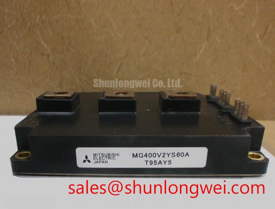
Do not infer the module’s substrate material from general packaging practice. Silicon nitride is one ceramic material discussed in thermal packaging, but the stated specifications here do not identify the internal substrate. For a replacement assessment, compare the mechanical drawing, terminal arrangement, mounting interface, and thermal requirements of the installed assembly. The MG200Q2YS40 can enter a specification comparison, but its voltage, current, topology, terminals, and mounting fit must be evaluated independently before considering interchangeability.
Benchtop Waveform Tuning: Gate Drive Isolation and Switching Stress
Capture the gate to emitter waveform at the module terminals while the opposing switch commutates, and look for unintended pulses or excessive ringing. A clean waveform at the driver output alone can miss voltage developed along the gate loop. As a Design Consideration, route the gate drive and its return as a close pair and keep them apart from the power commutation path. If the module provides a separate gate return terminal, establish its function from the terminal drawing before using it; the supplied physical specifications do not establish a Kelvin emitter connection.
Check the isolation barrier as a property of the selected driver, its power supply, and the assembled board, rather than assigning an isolation voltage or common mode transient immunity rating to the IGBT module. Observe both sides of the driver during switching to distinguish an input disturbance from a gate loop disturbance. Board clearances, isolation coordination, and acceptance tests depend on the equipment design and its applicable requirements. A drive that behaves normally at low bus voltage still needs evaluation under representative switching conditions before its noise immunity can be judged.
Where a drive uses a bootstrap supply, inspect its voltage through the longest commanded on interval and during repeated switching. Recharge opportunities, capacitor loss, and diode recovery can affect the available gate drive; their adequacy is determined by the chosen driver circuit and measured duty cycle. A similar separation helps when investigating diode commutation: compare current reversal and voltage ringing on the actual assembly instead of assigning an unverified reverse recovery characteristic to the MG400V2YS60A. These waveforms can also help locate a source of conducted or radiated noise, without implying that the module itself has an equipment level EMC approval.
MG400V2YS60A Operational Boundaries: Controlling Dynamic Gate Impedance
Measure the off state gate voltage while the complementary switch turns on, particularly if the drive reports intermittent cross conduction. Collector voltage change can couple through the IGBT’s reverse transfer capacitance and lift the gate; the resulting waveform depends on gate loop impedance, driver behavior, and layout. An active Miller clamp or negative off bias may be evaluated as a Design Consideration, but neither is an inherent module feature or a universal setting. The practical gate drive discussion in Evolution of Negative Off-Bias Gate Drive Circuits provides context for testing those options.
💡 Pro Tip: Keep opposing busbar current paths closely coupled to reduce turn off overshoot, then verify the collector voltage margin with switching measurements on the assembled equipment.
If changing gate impedance reduces ringing but raises switching loss, record both effects at the intended operating points before accepting the change. Compare gate voltage at the driver and module connections to reveal where loop voltage develops. For equipment with a braking chopper, inspect the chopper waveform and resistor path as a separate energy absorption subsystem; the MG400V2YS60A ratings alone do not establish braking energy capacity. Complete the assessment against the module’s 1200 V blocking and 400 A current ratings while keeping driver thresholds, thermal performance, and transient limits tied to the tested system.