
Content last revised on September 12, 2026
Preventing Spurious Faults: Optimizing Gate Drive Loop Geometry for MIG150J6CSB1W
| Specification | Official Product Data |
|---|---|
| Manufacturer | Toshiba |
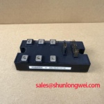
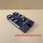
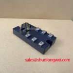
| Model | MIG150J6CSB1W |
| Category | IPM Intelligent Power Module |
| Rated Current | 150 A Official Datasheet Specification |
| Package | Toshiba Intelligent Power Module |
| Topology | General Power Stage |
| Rated Voltage | Not specified in the supplied official product data |
| Series | Standard |
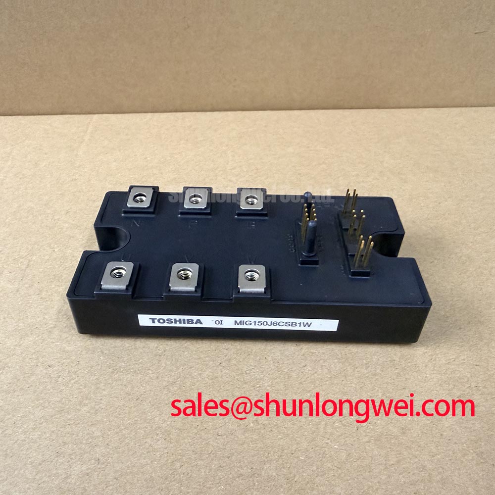
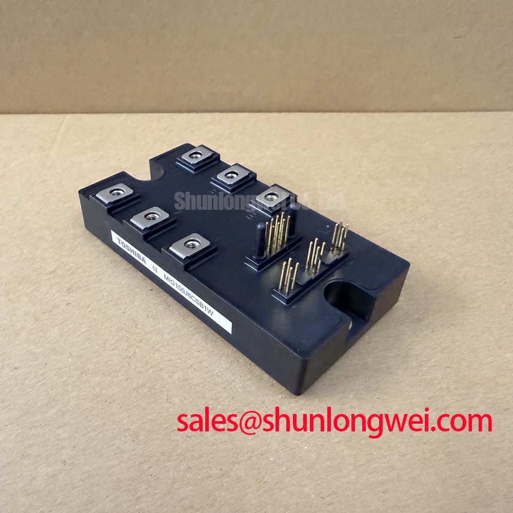
Measure the gate to emitter path with the power stage cold and disconnected, then compare the reading and polarity with a known good unit before applying a drive signal. The MIG150J6CSB1W is identified in the supplied official product data as a Toshiba IPM with a 150 A current rating, while its rated voltage and detailed terminal map are not provided here. Do not assign terminal functions from a visually similar module; use the original equipment drawing and the device marking to identify power, control, and auxiliary return connections.
A gate-drive loop should be treated as a compact switching circuit rather than as ordinary control wiring. The outgoing gate signal and its intended emitter return need a short, closely coupled route. The high-current emitter path should remain physically separate from the auxiliary gate-drive return so that load-current voltage drops do not appear as false gate signals. This separation is a Design Consideration for reducing emitter mutual coupling, unwanted feedback, and oscillation during turn-on or turn-off.
During a fault investigation, inspect the gate waveform directly at the module terminals instead of measuring only at the driver output. A clean driver-side waveform can become distorted by connector resistance, shared copper, via inductance, or a return path that runs beside a switching node. Use a differential probe with a suitable common-mode range and compare the gate-to-emitter waveform with the collector or phase-node transition. Ringing that changes when the probe ground arrangement changes may indicate a measurement-loop problem rather than a module defect.
The control board should keep sensitive logic traces away from the high-current commutation loop. Where the mechanical layout permits, route the auxiliary emitter return directly to the driver reference and avoid sharing that copper with current returning from the DC-link or motor phase path. Clearance should be established from the actual working voltage, pollution environment, insulation system, and applicable coordination analysis. The general principles of creepage, clearance, and insulation coordination are discussed in general electrical-insulation information; that reference should not be interpreted as a product-specific certification for this module.
High-side driver supply integrity also deserves a bench check. If the control circuit uses a bootstrap arrangement, evaluate the capacitor from the required gate charge, driver quiescent current, switching frequency, duty-cycle window, leakage, temperature, and the permitted supply ripple. The charging path must also tolerate the switching environment, and the bootstrap diode’s reverse-recovery behavior should be reviewed because recovery current can inject noise into the high-side supply. These are Engineering Recommendations for the surrounding driver circuit, not official electrical ratings of the Toshiba module.
If the drive board uses an optocoupler or digital isolator, check the isolation component’s common-mode transient immunity against the measured switching edge and confirm that its output does not momentarily enter an undefined state. A desaturation or fault line should be observed alongside the gate waveform, because a false protection event can result from control-ground movement, insufficient blanking, or supply disturbance. The presence of a power IPM does not establish the CMTI rating of an external isolator or the EMC compliance of the complete drive.
Thyristor trigger values such as IGT and VGT must not be assigned to this part. They are relevant only when a separate thyristor stage exists in the equipment. For any external thyristor interface, verify its own gate-trigger requirements and pulse-train behavior from the original documentation. For the MIG150J6CSB1W gate path, confirm the actual terminal polarity, driver reference, and protection sequence with the equipment schematic and an unpowered continuity inspection.
⚠️ Field Alert: Disconnect the DC link and control supply before removing or reseating the module connector, and maintain ESD protection during every cold-state comparison.
MIG150J6CSB1W Operational Boundaries: Evaluating Output Sinusoidal Filter vs dv/dt Reactor Limits
Capture the phase terminal waveform at the module output and at the motor terminals when long cable runs are present, then compare the two traces for overshoot and ringing. A cable can behave as a transmission line when its electrical length and impedance interact with the switching edge, producing reflected voltage at the motor end. Under unfavorable conditions, the terminal excursion can approach twice the local DC-link step, but the actual result depends on cable construction, termination, switching speed, motor impedance, grounding, and measurement bandwidth.
A sinusoidal filter and a dv/dt reactor solve different system problems. A sinusoidal filter is intended to reconstruct a smoother motor voltage and reduce high-frequency excitation, while a dv/dt reactor primarily limits the rate of voltage change and peak stress without necessarily creating a sinusoidal waveform. Selecting between them requires the motor insulation system, cable length, switching frequency, common-mode current, acoustic requirements, and thermal loss of the filter to be evaluated together.
When integrating the MIG150J6CSB1W into an electric forklift or warehouse traction inverter, designers should measure the complete output network rather than selecting a reactor from current rating alone. The module’s official supplied data confirms 150 A current capability, but it does not provide a voltage rating, switching-frequency limit, motor-cable limit, or filter compatibility value. Those boundaries must be verified from the original Toshiba documentation and the equipment design record.
The output filter must be placed so that its parasitic inductance and switching-node exposure do not create a second uncontrolled commutation loop. Keep the high-current conductors short, provide symmetrical phase routing where practical, and avoid allowing filter capacitors to return high-frequency current through sensitive control ground. A filter that appears effective at the motor terminals can still increase module stress if its resonance interacts with the PWM carrier or if damping is inadequate.
Bootstrap operation should be checked during the entire commanded duty-cycle range. The capacitor must supply the high-side driver’s gate-charge demand and quiescent current between refresh intervals while accommodating leakage, temperature variation, capacitor bias effects, and the current required by any protection circuitry. The bootstrap diode should be assessed for forward loss, reverse recovery, voltage stress, and charging-current loop inductance. Use the driver manufacturer’s equations and the original module documentation to calculate the required charge margin; a universal capacitor value would be an unsupported prescription.
For field troubleshooting, place voltage probes at the module phase terminal, filter input, filter output, and motor input where safe probing is possible. If the overshoot appears only after the reactor or filter is installed, examine impedance interaction and damping before attributing the symptom to the IPM. If the waveform changes with cable routing or motor frame bonding, investigate common-mode return paths and shield termination. A current probe can help separate normal motor current from high-frequency circulating current through the filter.
Forklift traction systems may operate with rapid load changes, regenerative braking, and repeated direction commands. Those operating conditions should be included in filter validation because a network that behaves acceptably during steady motoring can respond differently during regeneration. Protection thresholds must be coordinated with the measured phase-node peaks and the DC-link condition. The system engineer should verify peak margins during switching tests rather than relying on the nominal current value alone.
Benchtop Waveform Tuning: Mitigating Stress via DC-Link Capacitance Bank Layout and Low-ESR on MIG150J6CSB1W
Probe the DC-link directly across the module commutation path and compare the result with the voltage measured at the capacitor bank terminals. The difference reveals whether busbar inductance, capacitor spacing, or probe placement is contributing to an apparent spike. During turn-off, the overshoot is governed by the DC-link voltage, commutation-loop inductance, and current change rate; this relationship is commonly expressed in engineering analysis as the peak voltage rising with the product of stray inductance and di/dt.
Use a physically compact capacitor bank with a current path that follows the power terminals rather than a remote bulk-capacitor connection. Low-ESR capacitors can reduce ripple-related voltage movement, but ESR, ESL, ripple-current capability, temperature rise, and lifetime must be evaluated as a complete bank. A low-ESR component does not automatically correct excessive loop inductance or poor busbar geometry.
For laboratory tuning, begin with a low-energy current-limited setup and increase operating stress only while monitoring the DC-link, phase node, gate-to-emitter signal, and protection outputs. Use a differential probe with a short, controlled connection at the measurement point. Long probe leads can create ringing that is absent from the actual circuit and can lead to an incorrect snubber decision.
A snubber capacitor should be evaluated with its series resistance, pulse-current rating, voltage rating, placement, and heat dissipation. Its purpose is to control a measured transient, not to compensate for an oversized commutation loop. If a snubber reduces the visible spike but causes excessive repetitive current or heating, review the switching loop and capacitor-bank placement first. The final capacitance and damping values are system-determined and should be established from measured waveforms and thermal tests.
Symmetrical planar busbar geometry is a useful Design Consideration for reducing unequal current sharing and minimizing stray inductance. Keep the outgoing and returning conductors closely coupled where insulation coordination permits, maintain the required clearance from control circuitry, and avoid narrow necks around mounting holes or terminal transitions. The frequently quoted sub-25 nH target should not be imposed on this product without a validated layout model and switching test; the appropriate parasitic-inductance limit depends on the DC-link voltage, current, switching speed, clamp strategy, and module application.
Gate-loop damping should be tuned from the measured waveform. Excessive resistance can slow the transition and increase switching loss, while insufficient damping can permit oscillation and false protection activity. A suggested starting point may be used only for bench tuning after the driver output capability and gate-charge data are confirmed. The final setting belongs to the system design and must be checked at temperature, load, bus voltage, and regenerative operating points.
Do not infer the internal die-attach or packaging material from the external Toshiba Intelligent Power Module designation. General information about silver sintering and high-temperature die attach describes an industry process, not a confirmed internal construction detail of MIG150J6CSB1W. Thermal and electrical behavior should be judged from documented specifications and measured application data.
Assembly Integrity & Layout Architecture: Implementing Dynamic Power Loss Dissipation and Multi-R
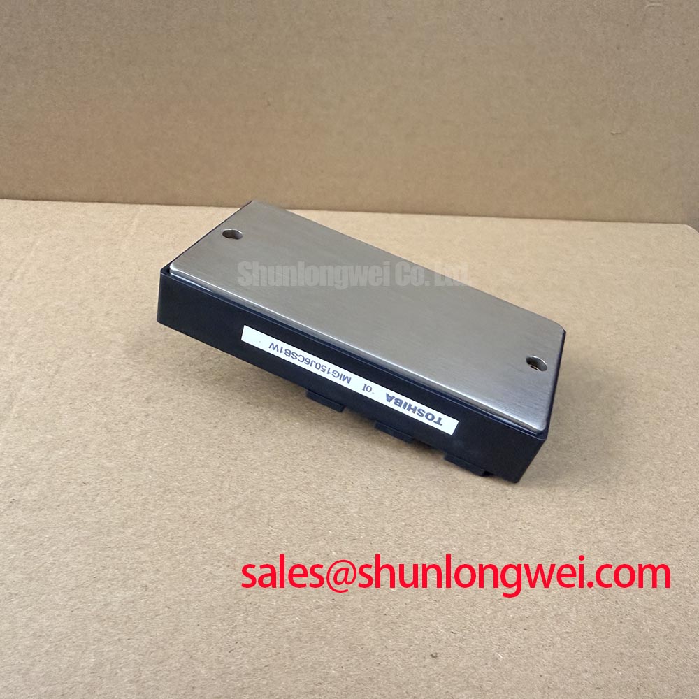
Inspect the mounting surface, terminal seating, fastener condition, and thermal interface before running a pulsed-load test. A nonuniform contact pattern can increase case temperature and create a misleading impression of excessive semiconductor loss. The supplied official product data identifies the package as a Toshiba Intelligent Power Module but does not provide a mechanical drawing, baseplate flatness limit, mounting torque, thermal resistance, or transient thermal impedance, so those values must come from the applicable Toshiba mechanical and thermal documentation.
Dynamic power loss should be separated into conduction loss, turn-on loss, turn-off loss, diode or freewheel behavior where applicable, and losses in the external filter or busbar. The correct calculation uses the actual current waveform, junction temperature, switching conditions, gate resistance, dead time, modulation pattern, and load power factor. A simple average-current estimate is insufficient for a traction inverter that repeatedly accelerates, brakes, and changes direction.
For pulsed overload evaluation, use the documented junction-to-case transient thermal impedance or multi-RC model associated with the exact device. The model represents heat moving through several time constants rather than appearing instantly at the case. Peak junction temperature must be calculated from the real power pulse profile and initial thermal state, then verified with case-temperature measurements and a suitable transient test. No operating lifetime, overload duration, or junction-temperature margin is asserted here because those figures require product-specific source data.
Thermal-interface application should be uniform and free of contamination, voids, trapped particles, and mechanical tilt. The heatsink should provide adequate stiffness and airflow for the complete assembly, including nearby capacitors, reactors, and switching conductors. If a cold-state electrical test passes but the module reports faults only after heating, correlate the event with gate supply movement, phase-node overshoot, heatsink temperature, and protection timing rather than assigning a single cause.
Multi-R thermal analysis should include the module, interface material, heatsink, enclosure, fan or natural-convection path, and ambient conditions. For equipment used in warehouse logistics, dust accumulation, restricted airflow, and frequent low-speed operation can alter the thermal boundary conditions. These are Design Considerations for the host system, not guaranteed environmental capabilities of the IPM. Altitude, cosmic-ray exposure, single-event burnout, FIT rate, insulation reliability, and safety certification also require authoritative device or system-level sources before numerical claims are made.
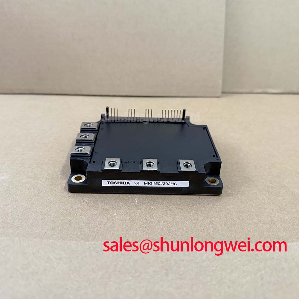
When evaluating a technically similar Toshiba power module for a repair program, compare the complete terminal arrangement, control logic, protection behavior, voltage class, thermal interface, and mechanical envelope rather than assuming interchangeability. The MIG150J202HC may be reviewed as a separate device for objective cross-reference, but no drop-in replacement is identified in the supplied product data. For structured bench procedures covering power-stage testing and failure analysis, consult the Field Engineer’s Handbook.
Record the cold-state gate-to-emitter observations, diode-test polarity, insulation test conditions, busbar waveform, case temperature, and protection response in the service report. This creates a repeatable acceptance baseline for the 150 A Toshiba MIG150J6CSB1W without converting an application-dependent measurement into an unsupported factory specification.