


Content last revised on September 29, 2026
Benchtop Waveform Tuning: Mitigating Stress via Dynamic Gate Impedance Control for Robust Operation of MIG75Q7CSB1X
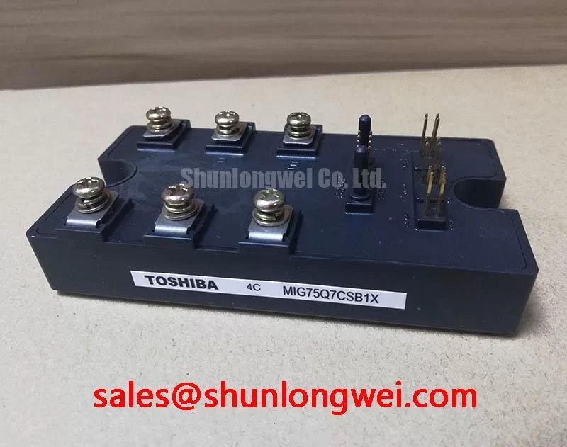
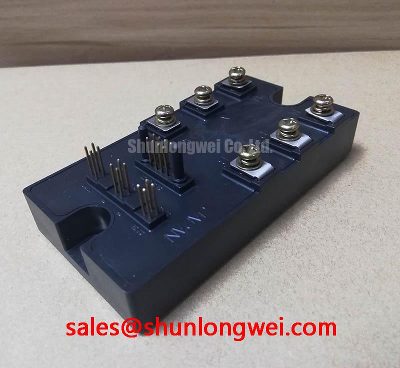
MIG75Q7CSB1X is a Toshiba intelligent power module (IPM). Its numerical voltage and current ratings, terminal assignment, dimensions and mounting limits are not specified in the supplied product data.
Probe the gate command and the corresponding power terminal waveform during a controlled switching test, looking for an unintended gate rise while the device is commanded off. On a drive board being assessed for MIG75Q7CSB1X, that comparison is more useful than adjusting a gate resistor from the symptom alone: a voltage rise at the gate can originate in coupling through the switching device, shared return impedance or a disturbance in the isolated driver supply.
With power isolated and stored DC link energy discharged, compare cold-state resistance between the identified power terminals against the service drawing and a known-good assembly. Check for a persistent short, inspect terminal hardware and photograph every control connection before removal. A multimeter can expose a gross fault, but it cannot establish switching health or prove that the gate driver is compatible. Obtain the Toshiba terminal drawing and electrical ratings before connecting a replacement to the drive board.
Design Consideration: A low-impedance active Miller clamp can help hold a device off when a neighboring switch produces a fast voltage transition. Whether the existing driver provides that function, and whether negative gate bias is appropriate, must be established from the module and driver documentation. Select gate impedance only after measuring turn-on and turn-off behavior across the equipment’s relevant operating conditions. A faster edge may reduce switching loss while increasing overshoot and disturbance at the isolated control interface; neither outcome can be settled by a bench waveform at one load point.
Trace the gate and return conductors as a pair. A long return path can make the voltage at the driver output differ from the voltage at the device terminals, particularly during rapid current changes. For an optocoupler or digital isolator, inspect the actual input, output and supply waveforms when the power stage switches. Common-mode transient immunity is a driver specification, not a property established by the IPM name. If the logic output changes unexpectedly, separate an isolation-stage disturbance from a gate-loop disturbance before changing either component.
For a forklift traction controller under compatibility review, repeat these checks with the original control board and its wiring arrangement. That equipment is a possible evaluation context, not an asserted application rating for this module. The system engineer must verify control timing, isolation behavior and switching margins against the original equipment requirements.
Benchtop Waveform Tuning: Mitigating Stress via Sizing Braking Resistors and Chopper Transistors on MIG75Q7CSB1X
Record DC link voltage during a controlled deceleration and compare it with the instant the controller commands its braking path. A rising link voltage calls for checks of the braking command, switching waveform, resistor continuity and connection integrity; it does not, by itself, identify a failed IPM. Trace the equipment schematic to determine whether the braking switch is part of the power module, elsewhere on the board or in a separate assembly. The supplied product data does not establish an internal braking transistor in MIG75Q7CSB1X.
Engineering Recommendation: Size the braking path from the machine’s measured deceleration duty, DC link behavior and the documented limits of its switch and resistor. Motor energy returned to the link must be absorbed or otherwise managed by the complete system. Check the resistor’s thermal installation and its protection circuit under the equipment manufacturer’s test procedure; a resistance reading at room temperature cannot establish its capacity for repeated braking events. Avoid substituting a braking resistor solely because it fits the mounting space.
Follow the power path from the input stage through the DC link before attributing repeated trips to the traction inverter. An SKIIP82AC121T1 may be assessed as a separate power-stage item when reviewing equipment topology, but its function and compatibility depend on the actual schematic. Inspect link connections, capacitor terminations and any surge-absorbing MOV network for visible damage or loose hardware. An MOV can participate in overvoltage protection, but its presence does not replace verification of braking control or switching peaks.
Where a repair calls for cross-model evaluation, compare the MIG30J103H against MIG75Q7CSB1X using manufacturer drawings for terminals, ratings, control interface, mounting and thermal limits. A similar product name is not evidence of an in-place replacement. Keep the original controller’s fault log and deceleration waveform with the comparison so that the selected hardware is evaluated against the fault that stopped the machine.
MIG75Q7CSB1X Operational Boundaries: Evaluating High-Frequency Commutation Loop Inductance Limits
Capture the turn-off voltage peak directly at the relevant power terminals, then compare it with DC link voltage measured during the same event. A large difference can point to inductive overshoot in the commutation path, although probe placement and bandwidth must be checked before treating the trace as a circuit result. Peak voltage depends on DC link voltage, loop inductance and the rate of current change; the allowable margin must come from verified device ratings and switching tests, not a generic loop-inductance target.
Design Consideration: Keep the outgoing and returning high-current paths close together to reduce loop inductance where turn-off overshoot threatens the device’s voltage margin. Inspect busbar alignment, capacitor connections and contact surfaces before changing snubber parts. A displaced conductor or loose connection can alter the measured waveform without any change to the module. Select snubber components from measured ringing and the system’s thermal and electrical limits, then repeat the test at conditions relevant to the equipment.
Separate the power commutation loop from the gate-control measurement. A probe ground lead that encloses a large loop can display apparent ringing that is partly a measurement artifact. Use a measurement arrangement suited to the circuit’s voltage and common-mode conditions, and compare the same points before and after mechanical work. If a clamp or MOV is present, check where it connects in relation to the observed peak; a protective part distant from the switching loop may not address the waveform seen at the device terminals.
Thermal mounting deserves the same physical inspection as the electrical path. Examine the mating surface, fasteners and cooling arrangement specified for the actual assembly; do not assume this Toshiba package uses flat-press disc springs or double-sided cooling. General packaging references on sintering and flip-chip interconnection describe manufacturing methods, but neither establishes the internal construction of MIG75Q7CSB1X.
For a broader discussion of how switching paths affect appliance power stages, see Resonant Topologies in Home Appliances. Its topologies are not specifications for this IPM. Use the equipment schematic and measured turn-off peak to decide whether a similar circuit principle is relevant to the repair.
MIG75Q7CSB1X Circuit Protection & Reliability: Calibrating Multi-Module Parallel Current Sharing
Measure current in each parallel branch during a controlled test and compare the waveforms at turn-on, steady conduction and turn-off. A branch that takes more current only during switching calls for inspection of gate timing, gate-return routing and busbar symmetry; a persistent steady-state difference also warrants checks of contacts, cooling and measurement calibration. Do not assume that a positive temperature coefficient of on-state voltage will balance these modules without Toshiba characteristic data for the operating region.
Inspect each module’s mechanical seating and the condition of its electrical joints before adjusting control settings. Unequal contact pressure or a disturbed cooling interface can change temperature and conduction behavior across branches. Follow the equipment’s mounting instructions for the actual package and fasteners rather than transferring a torque value from another module. ⚠️ Field Alert: Disconnect power and verify DC link discharge before loosening module terminals or probing cold-state resistance.
Design Consideration: Match gate-command paths and high-current paths as closely as the equipment layout permits when parallel branches must share switching current. Confirm the effect with branch-current and gate waveforms under controlled conditions; visual symmetry alone does not establish dynamic balance. If protection trips during acceleration or braking, compare its trip signal with the measured branch currents and link voltage before increasing a threshold. Protection timing and thresholds belong to the verified controller design.
For an in-place repair, record the original terminal mapping, heatsink contact arrangement, driver connections and fault indication alongside the replacement assessment. Check the module’s documented voltage, current, thermal and control-interface requirements against those of the machine. These checks define what still needs verification without treating a cold multimeter pass, a matching footprint or a brief unloaded run as proof of full-load compatibility.