
Content last revised on September 10, 2026
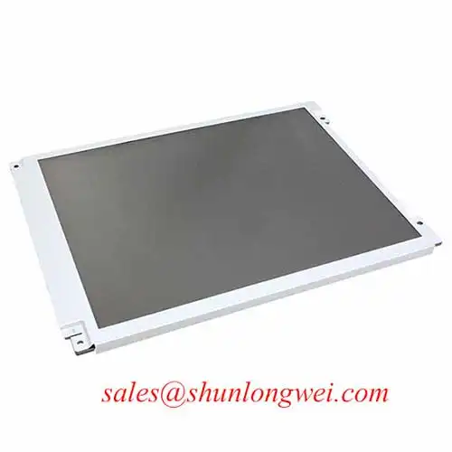
Begin bench verification of the NEC NL10276BC16-06 by measuring cold DC isolation resistance between the outer metal chassis frame and the signal ground planes with a calibrated insulation tester set to 50 VDC, ensuring impedance exceeds 50 MΩ before connecting power harnesses. In industrial plant floors, premature display degradation typically stems from thermal exhaustion, inadequate chassis sealing, or excessive mechanical clamping stress that alters the liquid crystal cell gap. Evaluating this 8.4-inch XGA (1024 × 768) module requires strict attention to interface grounding, backplane rigidity, and thermal dissipation paths across the entire assembly.
Suppressing Acoustic Capacitor Buzz & EMI Emissions across 200 Hz to 1 kHz PWM Frequencies
Backlight dimming circuitry operating within audio-frequency bands (200 Hz to 1 kHz) frequently induces audible acoustic noise due to inverse piezoelectric effects in multilayer ceramic capacitors (MLCCs). In original cold cathode fluorescent lamp (CCFL) configurations, strike voltages range from 1500 to 1650 Vrms (Official Datasheet Specification), demanding localized high-voltage isolation barriers and high-frequency resonant transformers. When transitioning or retrofitting these panels to solid-state constant-current LED drivers with wide-range PWM dimming (up to 1000:1 ratio), rapid switching of drive currents through input filtering capacitors creates cyclic mechanical expansion and contraction against the printed circuit board substrate.
To eliminate this acoustic resonance without shifting into electromagnetic compliance risk zones, field engineers must tune the PWM carrier frequency above the human auditory resonance peak (ideally 15 kHz to 25 kHz) if the integrated switching topology supports it, or replace standard barium titanate MLCC filter banks with metal-cap leaded ceramics or low-inductance aluminum polymer capacitors. Running PWM dimming within the baseline 200 Hz to 1 kHz band requires rigid component potting using neutral-cure electronic silicone to dampen acoustic transmission.
Mitigating high-frequency radiated emissions requires close control over differential signal routing. The single-channel LVDS digital interface carrying 6-bit or 8-bit RGB color information operates with high-speed transitions vulnerable to edge distortion and common-mode radiation:
- Differential Impedance: Traces must maintain a balanced differential impedance of 100 Ω ± 10% (Design Consideration for High-Speed LVDS Pairs) across the flexible flat cable (FFC) and receiver interface.
- Intra-Pair Skew: Physical length matching between positive and negative differential lines must remain tightly bounded, keeping intra-pair skew below 50 ps to prevent common-mode voltage conversion.
- Ground Return Loop: Shield braids must maintain continuous low-impedance termination directly to the chassis frame rather than bridging through high-impedance logic return pins.
Wide Temperature Operational Margin (-30°C to +85°C) & Sub-Zero Liquid Crystal Viscosity
Operating industrial liquid crystal assemblies in sub-zero machinery environments exposes liquid crystal fluid dynamics to significant viscosity increases. As the ambient operating temperature drops toward the lower operating boundaries of -20°C to -30°C, the kinematic viscosity of the nematic liquid crystal mixture increases exponentially. This physical change inhibits the rotational torque of liquid crystal molecules under an applied electric field, resulting in extended switching latencies between driving states.
| Operating Temperature State | Kinematic Viscosity Impact | Typical GTG Switching Speed | Engineering Mitigation Method |
|---|---|---|---|
| +25°C (Nominal Bench Ambient) | Baseline fluid dynamics | 20 ms combined rise/fall | Native LVDS single-channel drive |
| 0°C (Transition Threshold) | ~2.5x baseline viscosity | 45–60 ms response elongation | Look-Up Table (LUT) overdrive active |
| -20°C (Cold-Start Boundary) | ~8x to 10x baseline viscosity | 140–200 ms without thermal aid | Integrated transparent ITO heater & pre-heat phase |
When starting equipment in sub-zero environments, the observed response lag causes ghosting and contrast degradation on dynamic operator graphics. While look-up table (LUT) voltage overdrive provides pulse shaping that accelerates molecular reorientation at intermediate temperatures, extreme cold boundaries necessitate external thermal assist, such as laminated Indium Tin Oxide (ITO) front heater glass or localized PTC thermal pads, before full refresh rates are commanded. Thermal transition dynamics and seal degradation under extreme thermal shocks are documented extensively in the comprehensive Industrial Display & HMI Solutions engineering guide.
Repeated thermal cycling between -30°C and +85°C introduces mechanical stress across the perimeter epoxy sealing line. Because the coefficient of thermal expansion (CTE) of the borosilicate glass plates differs from that of the perimeter epoxy seal and outer metal frame, thermal ramps must not exceed 2°C per minute during environmental validation. Excessive ramp rates cause microscopic shearing along the perimeter seal, opening micro-channels that allow ambient moisture ingress, which eventually leads to internal polarization degradation and bubbling.
Surface Anti-Glare (AG) & Anti-Reflective (AR) Etched Coating for High Ambient Readability
Ambient illumination in bright industrial bays or outdoor operator cabs often washes out graphical data unless the front polarizer incorporates chemical anti-glare (AG) etching or multi-layer anti-reflective (AR) interference coatings. The NL10276BC16-06 features an integrated surface treatment designed to diffuse specular reflections, dispersing incoming pinpoint light sources across a wider scattering cone and maintaining readable contrast ratios without requiring excessive backlight drive levels.
Because this panel utilizes twisted nematic (TN) liquid crystal architecture, viewing angle orientation is asymmetric. The primary viewing direction exhibits stable contrast, whereas opposing angles introduce grayscale inversion where darker tones wash out or invert into high-luminance artifacts. When integrating this module into vertical console fixtures, technicians must align the optical axis to match the operator's line of sight, mitigating the contrast drop-off characteristic of non-IPS architectures.
Preserving panel optical uniformity requires disciplined mechanical mounting. Uneven compression around the bezel deforms the calibrated cell gap (typically 3 to 4 micrometers) between the front and rear glass substrates, causing visible light leakage along the perimeter, commonly known as optical edge mura.
| Mechanical Isolation Parameter | Recommended Specification Window | Failure Mode Mitigated |
|---|---|---|
| Bezel Compression Gasket Durometer | Shore A 30–40 (Closed-cell silicone) | Point-load shock wave transfer to glass edge |
| Target Gasket Compression Ratio | 25% to 35% nominal thickness | Loss of IP65 seal / Over-compression stress |
| Chassis Fastener Mounting Torque | 0.35 to 0.45 N·m (M3 thread class) | Mechanical frame twist & optical edge mura |
| Clearance to Rear Chassis Wall | > 2.5 mm air gap or thermal gap pad | Rear chassis deflection hitting backlight PCB |
⚠️ Maintenance Note: Verify that perimeter chassis fasteners are torqued strictly within 0.35 to 0.45 N·m in an alternating cross pattern, as uneven localized clamping induces mechanical frame twist and permanent optical edge mura.
Suppressing Pixel Jitter & Horizontal White Lines Induced by Adjacent 400V Motor Drives
Operating high-resolution display assemblies within the same physical enclosure as 400V variable frequency drives (VFDs) or heavy contactors introduces severe common-mode di/dt and dv/dt switching noise. In environments like heavy mining shovel & earthmoving equipment telematics displays, unshielded low-voltage lines easily pick up parasitic coupling from nearby IGBT switching transients. This interference manifests as horizontal sparkling white lines, erratic single-frame line tears, or loss of phase synchronization across the LVDS receiver.
The primary path for this interference is capacitive coupling onto the LVDS flat flexible cable (FFC) or high ground potential differences between the host rendering SBC and the panel interface board. To stabilize the signal against high EMI fields:
- Shield Termination: Enclose the LVDS wiring harness within a 360-degree tin-plated copper braid, clamping the shield directly to the chassis frame at both ends using conductive metal brackets rather than unshielded pigtail wires.
- Ferrite Attenuation: Position a split-ferrite core with high impedance between 100 MHz and 300 MHz over the input data harness adjacent to the panel connector, suppressing high-frequency common-mode noise currents.
- DC Ground Decoupling: Ensure the display logic return connects to the primary chassis ground through a low-inductance path, preventing common-mode transient currents from finding a return loop through the digital differential lines.
If legacy production machinery requires servicing and original panel inventory cannot be sourced during planned maintenance windows, technicians frequently evaluate the mechanically compatible NL10276BC30-24D as an alternative option, subject to pinout mapping and backlight driver circuit verification against plant enclosure envelopes.
Long-term luminance stability relies on constant-current driver performance. The backlight decay curve under nominal industrial temperatures exhibits an operational half-life target of 50,000 hours to 50% initial brightness (Official Datasheet Specification). Operating the illumination system above factory thermal limits accelerates phosphor degradation and shifts the white balance chromaticity coordinates toward blue-violet. Maintaining stable chassis ventilation pathways and verifying that digital clock margins do not drift outside setup-and-hold limits ensures the NEC NL10276BC16-06 maintains stable optical performance throughout severe industrial duty cycles.




