

Content last revised on October 18, 2026
Assembly Integrity & Layout Architecture: Implementing Baseplate Convexity Inspection for P639A75
I inspect the P639A75 mounting surface and heatsink contact area before disturbing the fasteners, recording uneven thermal compound transfer, trapped debris, and evidence of mechanical loading from the board. These observations help distinguish a contact problem from restricted cooling airflow. As a Design Consideration, check mounting surface flatness and any specified convexity against the mechanical drawing; a visual gap alone does not establish whether the module has an acceptable profile.
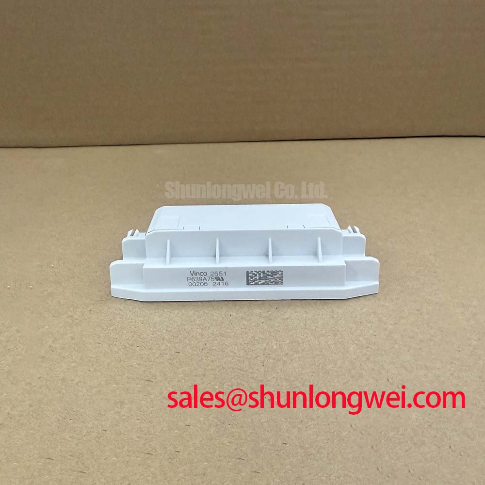
The Vincotech P639A75 combines converter, brake, and inverter functions in a PIM (CIB) arrangement. Its 1200 V / 15 A electrical classification, IGBT M7 silicon, and flow90 1 mounting architecture define the starting point for mechanical and electrical integration. The right-angle arrangement can reduce board footprint, but it also makes connector access, enclosure clearance, and board support relevant to serviceability. Keep external cable forces from loading the module connection area.
As an Engineering Recommendation, clean the mating surfaces and inspect them for burrs, embedded particles, or residual compound before assessing contact. Use the specified thermal interface material and application method. The required layer depends on surface geometry, compound behavior, and the approved assembly process; an arbitrary film thickness can conceal poor contact or leave excessive thermal resistance. Assess the compound transfer pattern during an authorized inspection rather than judging the joint from material squeezed around its edges.
Where the approved mounting procedure uses multiple fasteners, progressive diagonal tightening can help distribute clamping pressure. Use a calibrated tool and the torque assigned to the actual module and mounting hardware. Avoid pulling a misaligned assembly into position with its fasteners. Board support and heatsink alignment should allow the module to seat without bending the surrounding assembly.
Maintenance Note: At scheduled service, clear heatsink airflow paths and compare terminal and heatsink temperature trends under comparable loads before deciding whether the thermal interface needs inspection. As a Design Consideration, base the inspection interval on contamination, operating duty, and maintenance history. Check accessible power connections using their approved tightening procedure, and investigate moisture deposits or condensation before returning the assembly to service.
Assembly Integrity & Layout Architecture: Inspecting Reinforced Insulation Barrier Integrity for P639A75
Trace the isolation boundary from each driver output to the control circuit, including isolated power supplies, connectors, board slots, and contaminated surfaces. As a Design Consideration, reinforced insulation is a property of the evaluated barrier construction and its operating conditions. The P639A75 voltage classification does not establish a reinforced insulation rating for the surrounding driver assembly.
Review driver isolation specifications separately from common-mode transient immunity. Insulation withstand testing addresses a different requirement from a driver's ability to maintain the intended output during rapid changes in reference potential. Neither performance should be inferred from the module's blocking voltage. Inspect board clearances against the equipment's insulation design, paying particular attention to conductive dust, residue, damaged coatings, and moisture around isolation slots.
The JEDEC J-STD-020 Moisture/Reflow Sensitivity Classification addresses moisture and reflow sensitivity classification for nonhermetic surface mount devices. Its scope should remain separate from enclosure condensation control or reinforced insulation qualification. For this assembly, storage, soldering, cleaning, and drying practices should follow the applicable component and equipment instructions.
As an Engineering Recommendation, map the CIB power paths before modifying the input circuit. The converter section feeds the DC link, the brake section provides a switching path for the braking circuit, and the inverter section controls the output phases. Phase-angle conduction control requires a compatible controlled input stage; it should not be attributed to this module merely because the converter is integrated. Line-frequency ripple assessment belongs to the input supply, DC-link capacitance, loading, and control behavior considered together.
RC snubber evaluation should begin with the measured transient and the physical commutation path. As a Design Consideration, damping depends on circuit parasitics, component losses, and operating conditions. Place any selected network so its connections do not undermine its intended effect, then evaluate voltage peaks and heating across the equipment's operating range. Assigning component values from the module rating alone would leave the relevant circuit behavior unresolved.
When comparing power assemblies involving FP150R12KT4, examine its documented circuit arrangement before assigning it a front-end or auxiliary role. For broader topology context, the Ćuk converter inverting step-up/step-down topology describes a distinct conversion circuit; it does not describe the P639A75 CIB arrangement. Keeping those circuit identities separate helps prevent incorrect assumptions when tracing unfamiliar equipment.
Assembly Integrity & Layout Architecture: Preventing High di/dt Gate Loop Induced Transients for P639A75
Follow each gate connection back to its driver return and identify where load current shares the same conductor. The open-emitter arrangement supports access to the relevant emitter connections, but it does not by itself establish a dedicated Kelvin emitter terminal. Use the terminal diagram to distinguish available connections before changing a driver return or current measurement path.
As a Design Consideration, inductance shared by the load path and driver return can introduce a voltage during fast current transitions, altering the gate voltage seen by the device. Keep the intended gate drive loop compact and route its return with the corresponding gate conductor. Evaluate gate-to-emitter waveforms at the module connection using suitable probing, and compare the disturbance with collector current transitions. Probe placement and measurement loop pickup can otherwise obscure the behavior being investigated.
Apply the same attention to the DC-link commutation loop. Closely coupled outgoing and return conductors can reduce parasitic inductance and associated turn-off overshoot. The useful layout is determined by terminal geometry, insulation requirements, capacitor placement, and assembly access. Verify peak collector-emitter voltage under representative switching conditions while also checking the effect of any gate drive adjustment on losses and unwanted turn-on.
For context when comparing switching behavior across device technologies, The 1200 V CoolSiC™ MOSFET Advantage in Three-Phase Power Conversion provides a related discussion of three-phase power conversion. SiC behavior should not be transferred directly to the P639A75 IGBT M7 stage. Gate drive conditions and switching margins remain tied to the actual device, circuit, and measured waveforms.
As an Engineering Recommendation, assess parallel operation only where the equipment design supports it. A favorable temperature coefficient in part of an IGBT's operating range does not establish current sharing throughout operation. Static sharing depends on conduction characteristics and thermal conditions; dynamic sharing also depends on driver timing, connection impedance, and switching behavior. Compare branch currents and temperatures rather than inferring balance from a common gate command.
Desaturation protection also needs coordinated evaluation. As a Design Consideration, the sensing circuit must distinguish the normal turn-on transition from an abnormal collector-emitter voltage while the device is commanded on. Its blanking behavior, threshold, and soft turn-off response belong to the driver protection design. Check that shutdown limits the fault without creating excessive voltage overshoot, using the applicable short-circuit safe operating area conditions. The integrated NTC provides a thermal monitoring input; it does not replace fast electrical protection.
When assessing P639A75 compatibility for high-dynamics multi-axis CNC or robotics servo equipment, compare the terminal map, brake circuit, current sensing arrangement, cooling interface, and protection coordination. A cross-model review involving P084A2004 should use those same checks rather than assume interchangeability from package appearance. During controlled recommissioning, correlate gate waveforms, current feedback, NTC response, and driver fault records to resolve the specific mismatch before restoring normal duty.