

Content last revised on September 10, 2026
P760A06 Thermal Electrical Optimization: Common Mode Transient Immunity in Harsh Practical Tuning
| Manufacturer | Vincotech |
| Model | P760A06 |
| Product Category | IGBT Module |
| Rated Voltage | 600.0 V |
| Rated Current | 30.0 A |
| Package | flowPIM / flowPACK |
Measure the gate to emitter path and inspect the switching waveform with the inverter isolated from the DC link before changing any gate drive components. The P760A06 is a 600.0 V, 30.0 A Vincotech IGBT module in a flowPIM / flowPACK package, but the supplied production data does not establish a specific common mode transient immunity rating or reinforced isolation voltage for this model. Those values must therefore be confirmed from the original module documentation and the complete gate driver assembly rather than inferred from the voltage class.
In a compact industrial inverter or high speed CNC spindle drive, false turn on is often investigated by comparing the gate emitter waveform during the opposite switch transition. Use a differential probe with a suitable common mode rating and connect it at the module terminals, not several centimetres away on the driver board. A clean gate waveform at the driver output but an oscillating waveform at the module points toward the physical gate loop, connector arrangement, or return path. A disturbance visible at both locations requires wider checking of the isolation barrier, driver supply decoupling, control reference, and power commutation loop.
Gate loop inductance is controlled by reducing the physical area enclosed by the outgoing gate trace and its emitter return. Keep the high current collector and emitter paths away from sensitive gate control wiring, and route each channel as a tightly coupled forward and return path. If the module provides a separate auxiliary emitter terminal, the integrator should reserve that connection for the driver reference and keep it separate from the high current emitter path. The exact terminal function must be checked against the Vincotech mechanical and electrical documentation for the ordered configuration.
A gate resistor, ferrite element, or RC damping network should be selected only after observing the actual ringing frequency, peak gate voltage, switching loss, and driver output capability. Increasing resistance can reduce oscillation while slowing the switching edge and increasing dissipation. Reducing resistance can shorten switching time while increasing voltage overshoot and electromagnetic coupling. This is a Design Consideration, not a factory specification for P760A06.
Clearance and creepage around the isolation boundary must be evaluated against the working voltage, pollution environment, material group, enclosure design, and applicable safety standard. The component itself should not be described as independently certified for a complete inverter or CNC system. For practical switching verification, the guidance collected in IGBT Design & Integration can be used alongside the original Vincotech documentation and the system insulation design.
P760A06 Operational Boundaries: Evaluating SCSOA Overcurrent Protection and Implementing Limits
Capture the collector emitter voltage and gate emitter voltage together when testing an overcurrent event, then compare the turn off sequence with the driver fault signal. The available factory data for P760A06 confirms a 600.0 V voltage rating and a 30.0 A current rating; it does not provide a verified short circuit safe operating area, short circuit detection time, or integrated protection specification. A protection circuit must not be presented as part of the module unless the original technical document explicitly identifies it.
For field diagnosis, begin with a controlled low energy test and confirm that the current sensor, desaturation circuit, gate driver supply, and fault latch operate in the intended order. A delayed fault response may arise from sensor placement, blanking behavior, driver propagation delay, wiring inductance, or an incorrect gate clamp path. Measure the voltage directly at the module terminals because a remote probe point can hide the inductive rise that stresses the switch.
Two stage soft turn off is a possible Engineering Recommendation when the system topology and driver support it. The first action limits the current transition, while the following action completes turn off after the control circuit has assessed the fault condition. The timing, gate voltage levels, and energy handled during this sequence are system determined. The designer should verify the peak collector emitter voltage against the DC link boundary during fault testing instead of applying a generic detection time or gate bias value.
The freewheeling diode path also deserves attention during a high speed spindle drive investigation. Reverse recovery current can combine with stray inductance and raise the voltage stress seen by the switching device. Check the diode current commutation waveform, DC link ripple, busbar geometry, and local capacitor connection. A snubber can reduce ringing when its placement, parasitic inductance, dielectric behavior, and pulse energy are suitable, but its final values must be established from measured waveforms and loss calculations.
Radiated interference should be assessed at the system level. A semiconductor module cannot independently claim compliance with CISPR or EN 55011 because emissions depend on the enclosure, cable arrangement, filter, grounding, switching frequency, control board, and motor connection. Long motor cables may behave as transmission lines and produce reflected voltage at the motor terminals. Where a CNC spindle uses extended cable runs, the system engineer should evaluate the cable impedance, termination behavior, common mode current, and motor insulation stress with the complete installation.
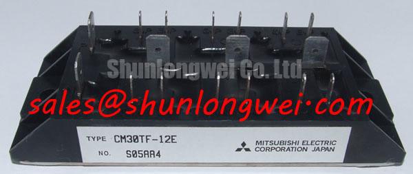
When a replacement assessment is required, compare the electrical topology, terminal arrangement, thermal interface, gate drive requirements, diode behavior, and mounting geometry rather than matching voltage and current alone. The CM30TF 12E may be reviewed as a separate, neutral cross reference for system evaluation, but substitution remains dependent on the original circuit, mechanical interface, protection settings, and validated switching tests.
Preventing Spurious Faults: Transient Thermal Impedance Guidelines for P760A06
Record the module case temperature and the duration of each overload pulse while monitoring current and collector emitter voltage; do not judge junction stress from a single steady state temperature reading. The confirmed rating for P760A06 is 30.0 A, yet the supplied product data does not include a transient thermal impedance curve, maximum junction temperature, overload duration, or ITSM specification. These missing limits must be taken from the applicable Vincotech datasheet before a pulse rating is calculated.
Transient thermal behavior is normally assessed with a junction to case thermal network represented by several time constants. Short pulses initially use the lower time constant portions of the network, while longer pulses progressively involve more of the case and heatsink path. In practical testing, obtain the device loss waveform from the switching current and voltage, apply the documented transient thermal impedance curve, and combine the result with the measured case temperature. The resulting peak junction estimate should then be checked against the manufacturer’s stated junction limit and the system’s required operating margin.
Do not replace a missing thermal impedance curve with a guessed fixed thermal resistance. A compact inverter may have a heatsink that appears cool while the semiconductor junction experiences repetitive thermal pulses. Switching frequency, modulation pattern, overload repetition, diode recovery, airflow, interface flatness, and neighboring heat sources all affect the result. Thermal calculations should therefore use the real mission profile or a documented worst case rather than only the nameplate current.
For a failed field unit, inspect the mounting surface, interface compound distribution, clamping condition, airflow path, heatsink contamination, and signs of localized discoloration. Compare the suspect phase with a known good phase using the same measurement method. A cold resistance check between relevant terminals can identify an obvious abnormal path, but it cannot confirm dynamic switching health, transient thermal performance, or insulation reliability. Use an oscilloscope and controlled load test when the static checks do not explain the fault.
Repeated overload recovery also requires attention to the freewheeling path and DC link. A high current pulse followed by incomplete commutation can create additional switching loss and raise the next junction temperature peak. Designers should verify the actual pulse sequence, cooling recovery interval, and protection response in the assembled inverter. Any claimed lifetime, failure rate, or safe operating duration requires a recognized source such as the original datasheet, qualification report, or applicable reliability publication; unsupported field figures should not be used for procurement decisions.
🔧 Field Alert: Disconnect the DC link and wait for the specified discharge condition before removing the module or gate driver connections, then follow the fastener and thermal interface instructions for the actual assembly.
Assembly Integrity and Layout Architecture: Suppressing Cres Induced Gate Voltage Spikes for P760A06
Probe the inactive switch gate at the module pins during the active switch transition and compare it with the driver reference before modifying the clamp circuit. A displacement current through parasitic capacitance can raise the inactive gate voltage, while shared emitter inductance can add a second disturbance to the measurement. The supplied P760A06 specification confirms the device category, voltage, current, and package, but does not confirm a specific Cres value, active Miller clamp function, or negative gate bias requirement.
Active Miller clamping is a possible Design Consideration where the selected gate driver supports it and the measured inactive gate excursion threatens the switching margin. The clamp loop should be physically short and referenced to the same emitter point used by the driver. If the driver uses separate turn on and turn off paths, verify that the diode, resistor, clamp transistor, and protection circuit do not create an unintended current path during reset or fault recovery.
Negative gate bias must not be assumed for this model. A value such as a negative five to negative fifteen volt range would be a driver design choice only when supported by the module’s gate oxide limits, driver isolation, fault behavior, and switching test results. The correct approach is to confirm the permitted gate emitter voltage from the original technical documentation, then validate both positive and negative excursions at the module terminals under the highest expected dv/dt condition.
Separate the power emitter and auxiliary emitter routing where the package provides both functions, and avoid allowing high di/dt current to share the gate reference conductor. Check solder joints, press fit contacts, terminal screws, busbar alignment, and connector strain because a mechanically sound module can still suffer from an electrically poor return path. Verify that the heatsink mounting force is even and that the module base is not twisted by an unsuitable fastener sequence.
When long motor cables are connected, inspect the inverter output waveform at the module, cable entry, and motor terminals. A reflected wave can produce a second voltage peak at the motor end, while common mode current can return through the shield, frame, bearing, or protective earth. Filtering and grounding decisions belong to the complete drive system. The reference material published by Mitsubishi Electric Global Semiconductor Device Technologies and its Power Semiconductors and High Power Modules section provides industry context for evaluating switching behavior, but it does not replace Vincotech data for P760A06.
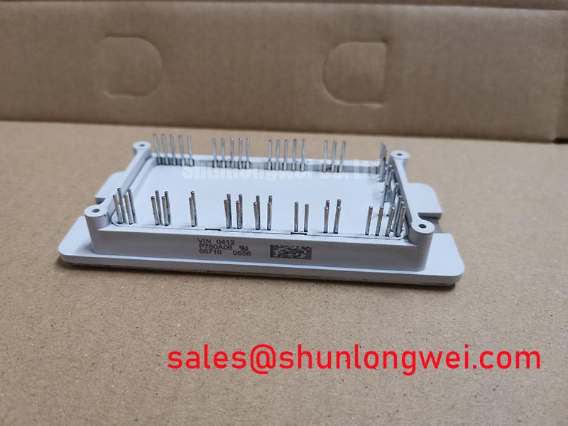
For procurement and emergency repair, record the complete marking, package form, terminal layout, failed phase position, measured static condition, and the original drive topology before ordering a replacement. The core identity to match is Vincotech P760A06, 600.0 V, 30.0 A, flowPIM / flowPACK IGBT module. Final acceptance should include a controlled insulation check, gate waveform inspection, current limited startup, thermal observation, and switching verification under the actual inverter load.