

Content last revised on September 20, 2026
Assembly Integrity & Layout Architecture: Implementing High-Frequency Commutation Loop Inductance for PM50CLA120
When the PM50CLA120 is evaluated for an industrial inverter welder or medium-frequency induction-heating power supply, the first layout check should follow the actual commutation path rather than the physical outline of the module. Trace the positive DC-link connection, switching terminals, return path, local film capacitor, and gate-driver return as one current loop. A long or asymmetric connection can add parasitic inductance and increase turn-off overshoot, ringing, and electromagnetic interference. The design objective is to minimize the high di/dt loop, while the final voltage margin must be verified with a suitable high-bandwidth differential probe during switching tests.
The relationship between switching overshoot and parasitic inductance can be considered in engineering terms as the DC-link voltage plus an inductive contribution related to loop inductance and current slew rate. This is an engineering calculation principle, not an additional PM50CLA120 datasheet rating. The measured peak must remain within the applicable device voltage boundary under the complete combination of bus voltage, load current, temperature, gate resistance, commutation speed, and wiring arrangement. A snubber capacitor or clamp network should therefore be selected from measured ringing energy and switching waveforms, not copied from a different module family.
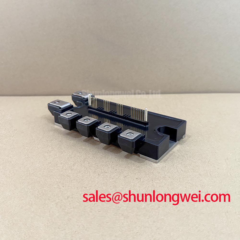
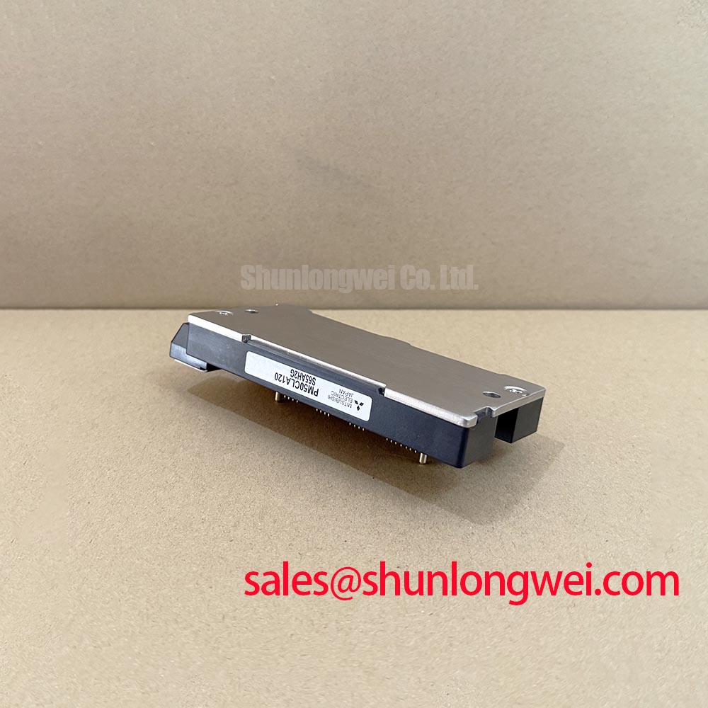
A practical assembly review should examine busbar symmetry, capacitor placement, terminal overlap, mechanical support, and insulation around the high-voltage path. Keep the power path compact and avoid routing sensitive gate-driver traces parallel to the collector or emitter bus for unnecessary distances. The required creepage distance and electrical clearance are system insulation decisions governed by working voltage, pollution level, material group, altitude, enclosure construction, and the applicable safety standard. They should not be inferred from the module name alone.
Long motor or transformer cables can behave as transmission lines. Reflections may produce a second voltage crest at the switching terminals, especially where cable impedance and load impedance are poorly matched. For a welding inverter or induction-heating supply, designers should measure the module terminal waveform at the real cable length and load condition, then evaluate filtering, damping, common-mode control, and switching speed as a coordinated system. A filter that reduces ringing at one operating point may increase losses or affect control response at another.
💡 Bench Tip: Compare diode-mode readings and gate-to-emitter resistance with a known-good cold reference using identical meter leads, polarity, discharge time, and ESD precautions.
For a neutral cross-reference discussion, engineers may also review the SKIIP37AC12T4V1, but electrical compatibility cannot be assumed from current or voltage labels alone. Terminal arrangement, switching behavior, protection functions, mechanical mounting, and the original control-board interface must all be checked before considering any alternative.
PM50CLA120 Thermal-Electrical Optimization: Cosmic Ray Robustness: Voltage Derating as a Practical Tuning Question
The 1200.0 V rating of the PM50CLA120 is an official product parameter, while the usable DC-link voltage in a finished machine is determined by switching overshoot, transient duration, temperature, load profile, insulation design, and the limits stated in the relevant datasheet. A voltage margin should be established through measured worst-case waveforms and documented operating conditions. It should not be represented as a universal percentage for every installation.
Cosmic-ray effects, single-event burnout, and altitude-related reliability require source-specific analysis. Neutron flux varies with altitude, shielding, geographic conditions, and operating exposure, while device susceptibility depends on semiconductor design and applied electrical stress. No FIT value, SEB threshold, altitude derating curve, or lifetime prediction is stated in the supplied product data, so a numerical failure-rate claim would be unsupported. Where the equipment operates above its normal installation altitude, the system engineer should request applicable manufacturer reliability data or conduct a qualified assessment rather than extrapolating from general semiconductor experience.
Protection coordination is more immediately testable in the workshop. Confirm the semiconductor fuse class, clearing behavior, prospective short-circuit current, and the fuse I²t against the module’s applicable surge and short-circuit withstand data. Fuse coordination is a system calculation: the protective device must clear the fault within the safe operating window while the module, busbar, capacitor bank, and enclosure withstand the resulting current and energy. The PM50CLA120 rating of 50.0 A must not be treated as a direct fuse-selection value, because continuous current, pulse current, cooling, switching frequency, and overload duration can produce very different semiconductor stresses.
For a dead-short investigation, first isolate the DC link and verify stored energy has decayed to a safe level. Then inspect the gate-driver supply, gate resistors, driver return path, and control interlock before applying a replacement module. A low-resistance reading between power terminals may indicate a damaged semiconductor path, but the meter result alone does not identify the original failure mechanism. Compare the result with a new cold reference and inspect the gate waveform on the surviving phase legs when safe test conditions are available.
The module may be used in a topology that includes a separate rectifier or front-end stage. The CM50DY-28H can be reviewed as a related system component, but its presence does not establish electrical interchangeability or a guaranteed front-end configuration for the PM50CLA120.
PM50CLA120 Operational Boundaries: Evaluating Thermal Time Constants and Peak Junction Limits
Thermal evaluation should begin with the actual loss profile rather than the 50.0 A nameplate value. Conduction loss, switching loss, pulse duration, repetition rate, case temperature, heatsink interface, airflow, and control strategy all affect junction temperature. The official data supplied for this page does not include a complete transient thermal impedance curve, maximum junction temperature, or detailed loss tables. Those values must be obtained from the applicable Mitsubishi Electric documentation before a peak-temperature calculation is completed.
A multi-RC thermal model can be used as an engineering calculation when the manufacturer provides the required thermal impedance data. The model applies the measured power pulse to the junction-to-case response and then adds the case-to-heatsink and heatsink-to-ambient paths. For a short overload, the instantaneous junction response may differ substantially from the steady-state result; for repeated pulses, thermal memory can accumulate. Designers should verify the worst-case temperature using the actual pulse train, not a single isolated event.
On the bench, mount the module using the manufacturer’s specified mechanical procedure and use a controlled interface layer suitable for the heatsink surface. Record case temperature near the defined reference location and correlate it with electrical loss measurements. A thermocouple attached far from the module case can lag the real condition, while an infrared reading may be affected by surface emissivity. These measurements are useful for comparison, but they do not replace the device’s specified thermal limits.
Surge-current evaluation also requires separation between a brief controlled pulse and an uncontrolled fault. The relevant ITSM or overload rating, if specified for the exact device, must be checked against pulse width, starting junction temperature, recovery interval, and the number of repetitions. A module that survives a single bench pulse may not have the same margin under repetitive welding current or induction-heating modulation. The control system should be tested for gate inhibition, fault reporting, and restart behavior before high-energy operation.
Thermal troubleshooting should compare all phases under the same load and cooling conditions. Unequal case temperatures can prompt inspection of mounting flatness, thermal interface consistency, current sharing, gate timing, and busbar symmetry. Such a temperature difference does not prove that one internal semiconductor element is defective; it identifies a condition that requires electrical and mechanical correlation.
Transient Dynamics & Electrical Design: Auxiliary Emitter Return Trace Separation on PM50CLA120
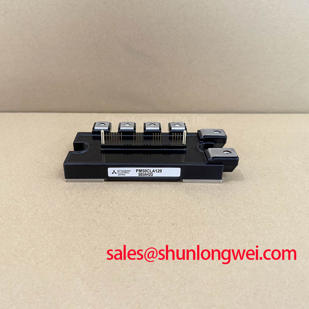
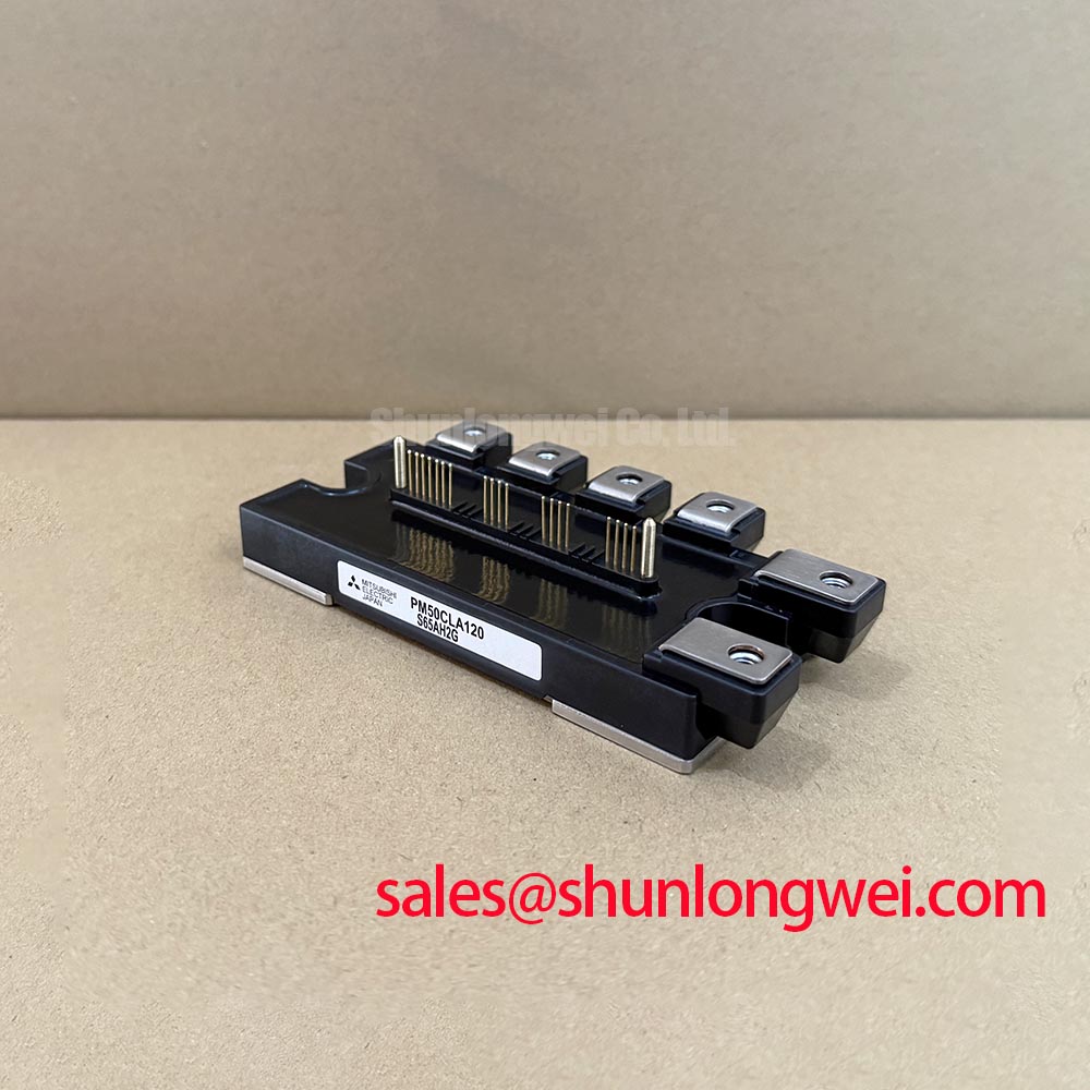
Where the installed PM50CLA120 terminal arrangement provides a separate auxiliary or driver return, the control return should be routed according to the manufacturer’s pin definition and kept distinct from the high-current switching return until the intended reference point. This is a design consideration, not confirmation that every physical variant contains a Kelvin emitter terminal. The applicable package drawing must be checked before assigning any terminal as an auxiliary emitter.
When gate-driver current shares copper with the main emitter current, the voltage developed across common impedance can appear as unwanted feedback at the driver reference. During fast commutation, that ground-bounce voltage may alter the effective gate-emitter drive and contribute to oscillation or uneven switching. The practical objective is to create a low-noise control reference, minimize shared path impedance, and place the gate resistor and driver return according to the actual terminal geometry.
Use a compact gate loop and keep the gate trace away from high-voltage switching nodes. Any negative turn-off bias, active Miller clamp, desaturation circuit, or isolated driver supply must be verified against the exact Mitsubishi documentation and the control board’s isolation strategy. The prompt does not provide a confirmed negative gate-voltage rating, so a specific negative bias value should not be prescribed. Common-mode noise should be measured at the driver reference during turn-on and turn-off events, with probe connections arranged to avoid adding a long measurement loop.
If oscillation appears on the gate waveform, inspect probe technique, gate resistance, driver output impedance, supply decoupling, auxiliary-return routing, and the power-loop waveform together. A ringing waveform may arise from several interacting parasitic elements, so replacing the module alone may not correct the condition. Verify the gate-to-emitter voltage at the module terminals, compare switching transitions across phases, and confirm that the control signal remains within the manufacturer’s stated electrical limits.
For broader context on switching-device technology and design tradeoffs, engineers can consult Wide Bandgap Revolution. The discussion is useful for understanding general high-speed switching behavior, but it does not change the silicon IPM specifications or operating limits of the PM50CLA120. Mitsubishi Electric’s global semiconductor technology resource should be used when confirming device-family information and documentation availability.