

Content last revised on October 4, 2026
FS50R12KT3 Operational Boundaries: Evaluating Common Mode Transient Immunity in Harsh Limits
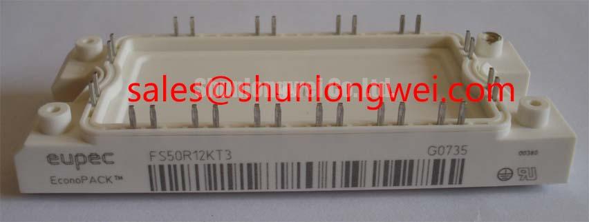
Before installing a replacement, isolate the inverter, inspect the module body and terminals, and verify the nameplate boundary of 1200 V and 50 A against the failed unit and the equipment service documentation. The FS50R12KT3 is an Infineon IGBT Module intended for evaluation in power conversion assemblies where the electrical ratings, gate drive arrangement, cooling method, and mechanical interface are confirmed by the system engineer.
The published product information available for this product identifies a voltage rating of 1200 V, a current rating of 50 A, and a Module package. These are Official Specification values for initial device screening. They do not, by themselves, confirm a particular common mode transient immunity value, reinforced isolation rating, creepage distance, or gate driver compatibility. Those properties must be checked in the applicable Infineon documentation and the complete inverter design.
For a commercial string inverter or microgrid energy storage converter, begin the service evaluation with the power stage isolated from the DC link. Check the module terminals for loose hardware, contamination, signs of localized heating, and mechanical movement. A cold resistance comparison between corresponding power paths can help identify an obvious short circuit or an abnormal open connection, but a resistance reading alone cannot confirm semiconductor health. When the result is unclear, compare the suspect assembly with an approved known good reference and continue with controlled semiconductor testing according to the service procedure.
Common mode disturbance is a system level issue. Gate driver isolation, driver supply decoupling, gate loop geometry, control reference routing, and switching node dv/dt all affect the possibility of an unintended gate voltage excursion. The FS50R12KT3 product rating does not establish a guaranteed CMTI value from the information supplied here, so a design team should not substitute an assumed figure for a verified datasheet specification. During commissioning, engineers should observe the gate to emitter waveform and the power switching node with properly rated differential probes while checking both turn on and turn off events.
Keep high voltage switching conductors physically separated from low level control and feedback wiring. Minimize the area of the commutation loop to reduce parasitic coupling, then verify the resulting peak voltage and ringing against the insulation and semiconductor limits specified for the complete assembly. The Infineon IGBT Modules Overview provides useful manufacturer level background for reviewing module construction, application conditions, and the relationship between the device and its surrounding power circuit.
When an inverter reports an intermittent gate fault, do not assign the symptom to the IGBT module without testing the driver output, isolated supply, interlock signal, and emitter reference. A waveform that differs from the corresponding healthy phase may indicate coupling, an unsuitable probing reference, driver malfunction, or a damaged power device. The correct next action is to compare the signal path under controlled conditions and verify the result with the equipment documentation.
Transient Dynamics and Electrical Design: Thermal Time Constants and Peak Junction on FS50R12KT3
The 1200 V and 50 A ratings provide the first screening boundary, not a complete operating point for a pulsed inverter. Actual junction temperature depends on conduction loss, switching loss, pulse duration, duty cycle, case temperature, heatsink performance, interface quality, and the thermal impedance data specified for the exact device revision. A thermal RC model can be used as an Engineering Calculation only after those manufacturer parameters and the converter load profile are available.
For field replacement work, inspect the mounting surface before fitting the module. It should be clean, flat, and free from burrs that could distort the baseplate. The thermal interface material should be applied as a uniform thin layer suitable for the selected heatsink and installation method. A commonly used industry starting range of approximately 50 to 80 micrometres may be treated only as a Design Consideration, not as an FS50R12KT3 Official Specification. The system builder must follow the material supplier instructions and validate the resulting thermal resistance.
Use a progressive cross pattern when tightening multiple mounting points so that the baseplate seats evenly. The correct torque is determined by the fastener size, module construction, washer arrangement, heatsink specification, and manufacturer instructions. If the original assembly documentation is unavailable, the maintenance team should obtain the applicable mechanical drawing rather than applying a guessed torque value. After installation, inspect for rocking, uneven contact, displaced interface material, and distortion around the fixing points.
⚠️ Field Alert: Disconnect the DC link and gate drive supplies before handling the module, and follow the equipment procedure for verifying that stored energy has fallen to a safe service condition.
During overload investigation, record case temperature, switching frequency, load current, ambient conditions, and the duration of the event. A brief overload may produce a different thermal response from a repeated pulse sequence even when the average current appears similar. If the module trips after warmup, inspect the cooling path, fan or pump operation, heatsink contact, and temperature sensing circuit before attributing the event to an internal semiconductor failure.
The Infineon IGBT paralleling application note is relevant when a converter uses more than one power module. It explains why current sharing, wiring symmetry, gate control, and dynamic switching behavior must be assessed together. It should be used as an engineering reference rather than as evidence of an unlisted electrical or thermal rating for this particular model.
Assembly Integrity and Layout Architecture: Implementing Derating Guidelines and Mismatched Parameters for FS50R12KT3
Static current sharing between parallel IGBT paths is influenced by conduction characteristics, temperature, wiring resistance, and the balance of the external circuit. A positive temperature coefficient of conduction voltage can support current sharing in some operating regions, but the presence and usable range of that behavior must be confirmed from the exact manufacturer curves. It should not replace thermal measurement or dynamic current verification.
When engineers evaluate the FS50R12KT3 in a commercial string inverter or microgrid storage converter, each parallel path should have a closely matched physical route from the DC link through the module and back to the switching return. Keep the gate drive paths similar in length and impedance, and avoid routing one gate loop beside a high current commutation path while another runs through a quieter region. These are Design Considerations intended to reduce mismatch; the final layout remains system dependent.
Check the gate resistor arrangement, driver output capability, isolation structure, and protection timing against the original equipment design. The supplied product data does not confirm a specific gate threshold, gate charge, short circuit withstand time, internal thermistor configuration, or terminal assignment. The system integrator should verify every one of these details from the correct manufacturer datasheet and mechanical drawing before applying a replacement.
For procurement and repair screening, record the part number, brand, package style, rated voltage, rated current, and the equipment position from which the failed unit was removed. A model with a higher current number is not automatically a compatible substitute because switching characteristics, pin arrangement, gate requirements, thermal interface, and fault protection may differ. The FS100R12N2T4 can be reviewed as a separate Infineon module option, but its suitability must be established through a full electrical, mechanical, thermal, and control interface comparison.
Derating is also determined by the complete converter. The DC link voltage, modulation method, switching frequency, load profile, enclosure temperature, airflow, altitude, and protection response all influence the usable margin. Since no specific derating curve or field lifetime data is established here for the FS50R12KT3, engineers should calculate the expected stress from verified manufacturer curves and confirm peak conditions by measurement. Avoid treating a nominal 1200 V rating as permission to operate at that value continuously under every switching transient.
Benchtop Waveform Tuning: Mitigating Stress via PCB Symmetry Considerations for Dual IGBT on FS50R12KT3
Waveform testing should start with the equipment in a controlled low energy condition, using measurement instruments and probes rated for the expected common mode and differential voltage. Confirm probe compensation and reference placement before interpreting ringing. An apparently abnormal gate waveform can be created by a long probe ground connection or an unsuitable reference point, so the measurement method must be checked before changing the gate network.
Where the module and driver provide a separate auxiliary emitter or control return, keep that return associated with the gate driver reference and separate from the high current emitter path as required by the verified terminal arrangement. The purpose is to reduce voltage developed by load current through shared parasitic inductance. This recommendation is conditional because the actual internal terminal configuration and pinout must come from the official mechanical and electrical documentation for the device revision.
During bench tuning, compare the gate to emitter waveform at the module terminals with the driver output measured at the driver board. If the signals differ, inspect the interconnect, auxiliary return, isolation supply, and local decoupling. If both are similar but the switching node shows excessive ringing, examine the commutation loop, busbar arrangement, snubber network, and measurement setup. The corrective choice should be based on measured peak voltage, switching loss, thermal response, and the limits of the complete power stage rather than on a generic resistor or damping value.
For dual device arrangements, maintain symmetry in the power path and gate control path wherever the topology requires parallel operation. Avoid placing one device closer to the DC link capacitor while routing the other through a longer return path. After any layout or wiring change, repeat turn on and turn off measurements across the expected load range and check the case temperature of each module separately. A difference between devices may result from routing, driver timing, thermal contact, sensor position, or device characteristics, so diagnosis should remain measurement based.
The broader design implications of fast switching technologies can be reviewed in Wide Bandgap Revolution. That reference is useful when comparing system level switching behavior and layout challenges, but it does not change the verified identity or ratings of the FS50R12KT3. For a replacement decision, confirm that the original equipment requires an Infineon 1200 V, 50 A Module, then validate the terminal layout, gate drive conditions, cooling interface, protection coordination, and measured switching performance before returning the inverter to service.