

Content last revised on November 13, 2026
QF15AA60 Thermal-Electrical Optimization: Power Factor and Harmonic Mitigation
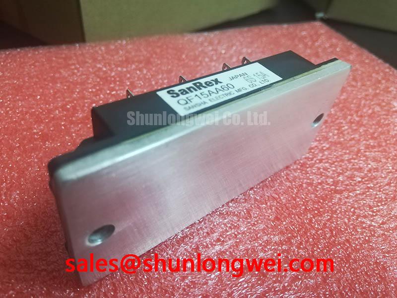
I check the power-terminal connections against the equipment schematic before investigating poor power factor or changing control commands. The QF15AA60 is a SanRex (Sansha Electric) power transistor module in the 600 V, 15 A class, not a thyristor/diode module. Consult the manufacturer datasheet for the definitions and operating conditions of these ratings, terminal drawing, mounting requirements, and protection characteristics before approving a replacement.
Design Consideration: Input power factor depends on the complete converter architecture, not simply on the transistor module. Establish whether the QF15AA60 operates in an inverter, chopper, or another switching stage, and identify the equipment’s input rectifier and any power-factor-correction circuitry. I compare control commands with measured supply voltage, input current, and converter output rather than assuming a direct relationship between the module’s switching commands and input power factor.
A power analyzer should separate displacement power factor from total power factor before anyone adjusts compensation. Harmonic mitigation belongs to the complete converter: first check input-stage operation and phase balance, then assess line impedance and existing filters against measured current harmonics. Adding capacitance without checking resonance can complicate the original fault.
Engineering Recommendation: Assess cooling alongside these measurements. Inspect heatsink flatness, contact cleanliness, thermal-interface coverage, and fastening condition. Use the specified mounting sequence and torque, with interface thickness determined by the approved assembly instructions. For changing load duty, evaluate pulse heating through the applicable transient thermal impedance, Zth, rather than relying only on average current.
Field Alert: Do not substitute terminal-tightening torque for baseplate mounting torque; follow the specified requirement for each joint.
QF15AA60 Operational Boundaries: Evaluating Commutation and Reverse Recovery
Capture commutation current and device voltage together when investigating a recurring recovery spike. Use probes with suitable voltage capability, bandwidth, and common-mode performance, and keep measurement connections short enough to distinguish circuit ringing from probe artifacts. Record load, temperature, and switching conditions so that comparisons describe the same operating point.
Design Consideration: Peak reverse recovery current, reverse recovery charge, and recovery time describe different aspects of diode commutation. Identify the diode carrying the commutating current in the actual circuit before attributing a recovery waveform to the module. Recovery time alone does not establish softness: the current-decay shape and its interaction with circuit inductance influence overshoot and ringing. These quantities also depend on test conditions, so a waveform captured elsewhere is not a QF15AA60 acceptance limit.
Compare measured transistor voltage excursions with the applicable collector-emitter voltage limit and safe operating area in the QF15AA60 datasheet. The 600 V voltage class must not be treated as a repetitive peak reverse-voltage rating or a recommended operating voltage. Manufacturer product documentation from SanRex Sansha Electric Power Semiconductor Modules is the appropriate authority for device-specific characteristics and test conditions.
Engineering Recommendation: Coordinate fuses using the manufacturer’s applicable semiconductor withstand information, the fuse’s total-clearing characteristics at the actual fault voltage, and prospective fault current. Pre-arcing I²t alone does not describe the full interruption event. Check the fuse manufacturer’s coordination tables and clearing curves; the module’s current rating is not a short-circuit protection specification. A fuse does not replace fast electronic fault protection, and fuse coordination does not establish enclosure containment.
For broader switching-material context, Si vs. SiC vs. GaN explains relevant loss mechanisms. Apply that background to waveform interpretation, not as evidence of interchangeable recovery behavior or additional QF15AA60 ratings.
Field Diagnostics & Commissioning: RC Snubber Network Optimization in QF15AA60 Circuits
Inspect the existing snubber connections and compare measured voltage edges with the intended switching sequence before changing resistance or capacitance. An unexpected conduction event may involve drive interference, switching transients, timing errors, or an external current path; the symptom alone does not identify the cause.
Design Consideration: An RC snubber can limit voltage slew and damp oscillation, but its capacitor also stores energy that must discharge through the surrounding circuit. Select resistance and capacitance using measured ringing, repetitive pulse energy, resistor dissipation, and the device’s applicable switching limits. Final values require validation across the equipment’s operating range, including restart and load transitions.
A series saturable reactor should be assessed only where the converter design calls for current-rise control. Its saturation behavior, reset conditions, and thermal duty affect commutation. Likewise, coordinate an existing MOV network with normal voltage excursions, clamping behavior, absorbed energy, and upstream protection rather than choosing a suppressor from the module’s voltage rating alone.
Engineering Recommendation: During replacement assessment, compare terminal functions, circuit arrangement, mechanical fit, cooling requirements, safe operating area, and drive compatibility. A separate device such as PDMB75E6 requires its own comparison; its inclusion in a sourcing search does not establish interchangeability.
When evaluating the QF15AA60 for a medium-frequency induction melting or hardening furnace, establish its exact role in the original power circuit before substitution. Commission against the equipment’s approved procedure, checking switching timing, commutation overshoot, protection operation, and thermal behavior before returning the assembly to service.