



Content last revised on September 21, 2026
STE07DE220 Operational Boundaries: Evaluating Thermal Paste Degradation and Operating Limits
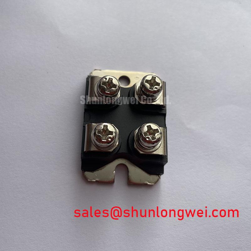
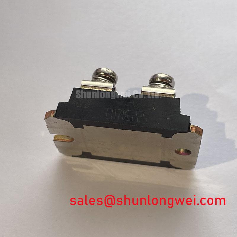
The STE07DE220 is identified with a 600 V voltage rating, a 7 A current rating, and an ISOTOP / Max247 package. These official values establish the starting electrical boundary for repair assessment, but they do not replace verification of switching waveform peaks, load current shape, heatsink condition, or the original equipment protection strategy.
For a heatsink mounted assembly, thermal interface condition deserves inspection before electrical commissioning. Dried paste, uneven contact pressure, particulate contamination, and trapped air can raise the thermal resistance between the package mounting face and the heatsink. As a Design Consideration, technicians commonly control thermal interface material as a thin, continuous layer, typically within a 50 to 100 µm range where the mechanical stack permits it. The objective is coverage and void reduction rather than building a thick insulating layer.
Check the heatsink mounting plane for burrs, surface damage, residue, and local curvature. A slightly uneven mounting surface can create concentrated loading on one area of the package while leaving another area thermally isolated. Where multiple fasteners are used, tighten them sequentially and progressively so the package settles evenly. The applicable fastening hardware, torque requirement, insulation arrangement, and creepage clearances must be verified from the original mechanical drawing and service documentation.
💡 Pro Tip: Apply thermal compound only after both contact faces are cleaned, then verify even package seating before applying final fastener torque.
A thermal complaint should not be assigned to the STE07DE220 on appearance alone. Measure heatsink airflow, examine fan operation, inspect thermal compound condition, and compare switching behavior with a known healthy power stage where available. A recurring overtemperature trip may also relate to control timing, an overloaded output, an impaired rectifier section, or insufficient cooling capacity in the enclosure.
Assembly Integrity & Layout Architecture: Suppressing 2× VDC Voltage Doubling for the STE07DE220
Long output cables can behave as transmission paths rather than simple conductors during fast switching transitions. Under certain cable length, load impedance, and switching edge conditions, reflections can produce terminal excursions approaching twice the DC link voltage. This is a system phenomenon, not an official switching capability claim for the STE07DE220. Engineers should capture the relevant terminal waveform with suitable high voltage differential measurement equipment and verify peak voltage margin against the 600 V official rating.
In industrial inverter welder and medium frequency induction heating equipment, the DC link, switching device, output choke, resonant network, and cable arrangement must be evaluated as one commutation path. A dv/dt filter or output choke can be considered where measurement indicates cable reflection or load side stress. Component selection must account for the actual operating frequency, current waveform, insulation requirement, heat dissipation, and control response of the existing equipment.
Minimizing parasitic inductance in the high current commutation loop is a Design Consideration for suppressing turn off overshoot. Keep the DC link capacitor connection, bus conductors, and switching path physically compact and mechanically stable. Film snubber capacitors, where included by the original topology, are generally most effective when placed close to the loop producing the transient. Their capacitance, voltage capability, pulse current rating, and connection geometry must be determined from measured waveforms and the equipment design.
A metal oxide varistor can contribute to coordinated surge handling in an appropriate network, but it is not a substitute for controlling repetitive switching overshoot through layout. Likewise, the reverse recovery behavior of the companion freewheel diode can affect ringing and conducted noise. The installed circuit should be reviewed for diode recovery characteristics, snubber condition, gate timing, and DC link capacitor integrity before altering any suppression component.
For upstream or associated power stage assessment, the SKM100GB063D can be reviewed as a separate complementary power semiconductor reference. Electrical topology, package interface, ratings, cooling arrangement, and drive requirements must be compared independently before any service decision.
Field Diagnostics & Commissioning: Differential Gate-Emitter Loop Routing in STE07DE220 Topologies
Before applying power, inspect the original schematic and terminal marking to establish the actual function of every connection in the installed assembly. The published basic identification for STE07DE220 confirms the voltage, current, and package values stated above, but system integrators should verify terminal function and drive connection from the original panel documentation. No gate pin arrangement, auxiliary emitter connection, or internal topology should be assumed from the package style alone.
Where the surrounding inverter topology uses a gate-driven switching device, the driver return path should be examined separately from the main high current return. Shared inductance between a power current path and a control reference can disturb the gate-to-emitter signal during switching. That disturbance may appear as ringing, irregular turn-on behavior, apparent false triggering, or unexplained variation between otherwise similar phase legs. Oscilloscope measurements should use a probing method appropriate to the voltage and isolation conditions.
Designers should route the control reference as a low loop area path and keep it separated from the high di/dt power return wherever the circuit architecture provides a dedicated reference terminal. This is a Design Consideration intended to reduce mutual coupling, not an official STE07DE220 package claim. The effectiveness of a revised routing arrangement must be verified during switching tests at the system’s intended DC link voltage and load condition.
Driver isolation also requires system level review. Optocouplers and digital isolators are selected according to the actual common mode transient environment, supply arrangement, propagation timing, insulation coordination, and controller logic. Do not infer device level EMC compliance from the STE07DE220 itself. Equipment compliance depends on the complete enclosure, cable system, filtering, grounding, switching behavior, and test configuration.
Current feedback can assist commissioning when it is correlated with the switching waveform and load condition. Hall based sensing is commonly used for isolated industrial current measurement, while magnetoresistive sensing is another established measurement approach. Engineers reviewing sensing options can consult Hall effect sensor principles and giant magnetoresistance sensor principles as general technical references. Sensor choice remains dependent on the required bandwidth, isolation arrangement, conductor geometry, and calibration method.
For broader review of gate drive routing, thermal paths, and switching loop behavior, see IGBT Design & Integration. That technical material should be used alongside the original machine schematic and measured operating data.
STE07DE220 Operational Boundaries: Evaluating Thermal Cycling Margins and Braking Limits
Motor deceleration and rapid load energy release can elevate DC link voltage when energy returns from the load into the supply bus. In equipment using a braking arrangement, the braking semiconductor, ballast resistor, DC link capacitor, and control threshold act together. The basic STE07DE220 information provided does not establish an internal braking function, braking energy rating, or braking resistor compatibility. These functions must therefore be confirmed from the original inverter schematic.
When troubleshooting a DC link overvoltage event, inspect whether the braking command is present, whether the braking path is electrically continuous, and whether the ballast resistor shows mechanical or thermal damage. A missing braking command can originate in the controller, feedback circuit, interlock chain, or power supply section. A damaged resistor may be associated with prior overload, insufficient cooling, connection deterioration, or repeated energy absorption beyond the installed system design.
Thermal cycling assessment should focus on actual operating conditions rather than assumed lifetime figures. Review duty cycle, ambient condition, cooling performance, load inertia, switching behavior, and the measured temperature rise of accessible system components. No specific lifetime, failure rate, safety certification, altitude derating, or insulation reliability claim should be inferred from the available STE07DE220 basic specifications.
A semiconductor fuse may be coordinated with a power stage to limit fault energy, but the correct fuse selection depends on the circuit’s prospective short circuit current, protection timing, allowable I²t, and coordination with contactors or electronic protection. Verify these conditions against the equipment design rather than selecting by nominal current alone. Where a replacement assessment is required, the P950A may be reviewed as a separate candidate reference, subject to full confirmation of electrical ratings, topology, package fit, terminals, thermal interface, and drive compatibility.