Content last revised on September 10, 2026
RM500CZ-M Inspection and Integration Overview
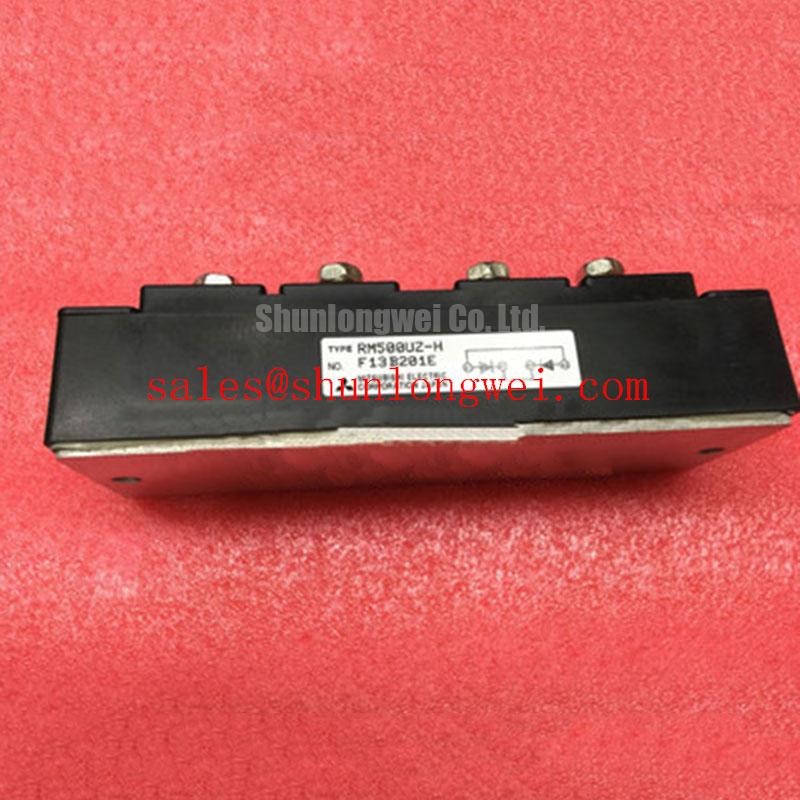
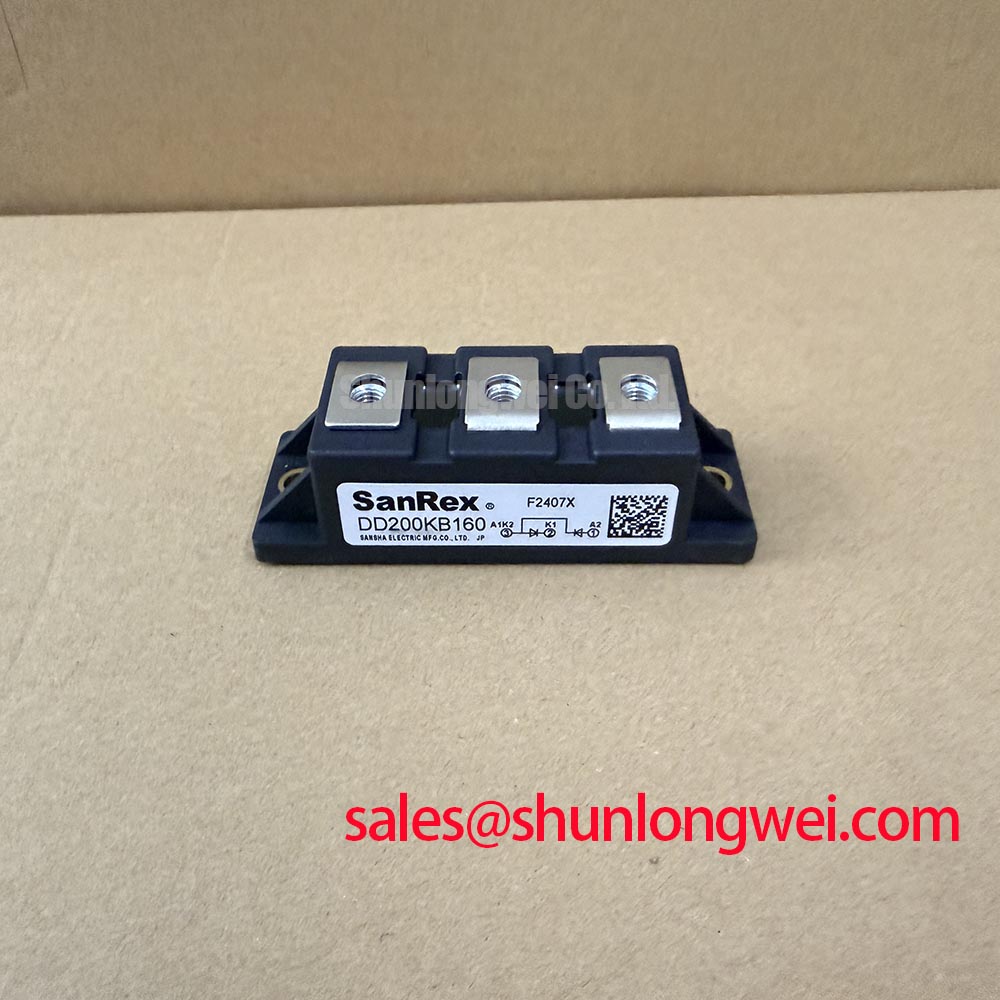
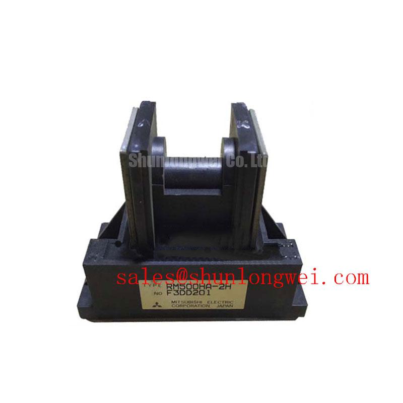
Before fitting the RM500CZ-M, isolate the cabinet and compare the module marking, terminal arrangement, baseplate condition, and connected circuit position against the original service documentation. Mitsubishi Electric identifies this unit as a Diode Module with a Standard Industrial Rating working-voltage classification and Standard Operating Current classification. The system integrator should obtain the original module documentation before approving voltage, current, thermal, or protection coordination for a replacement installation.
This product page addresses practical inspection and integration of the RM500CZ-M in power conversion assemblies. A diode module has no gate terminal or gate-trigger specification, so IGBT gate resistance, thyristor firing current, dead-time settings, and gate pulse sequencing belong to the surrounding converter hardware rather than to this module itself. For manufacturer-level context on high-power semiconductor products, consult Mitsubishi Electric Power Semiconductors & High-Power Modules.
| Identification Item | Declared Classification | Specification Status |
|---|---|---|
| Product model | RM500CZ-M | Official product identification |
| Manufacturer | Mitsubishi Electric | Official manufacturer identification |
| Product category | Diode Module | Official product classification |
| Working voltage | Standard Industrial Rating | Official supplied classification |
| Operating current | Standard Operating Current | Official supplied classification |
RM500CZ-M Mounting and Heatsink Contact Pressure
Start the mounting assessment with the heatsink rather than the circuit. Remove residual thermal interface material from the contact surface, then inspect the module baseplate seating area and the heatsink for raised debris, corrosion, burrs, local dents, or uneven machining marks. Any local high point can restrict contact area, create uneven pressure, and lead to localized thermal stress during load cycling. The RM500CZ-M should sit flat before fasteners are tightened; it should not be pulled into position by the mounting hardware.
Thermal resistance from junction to case is an Official Datasheet Specification only when the applicable Mitsubishi Electric documentation provides the associated test condition and value. It should not be estimated from case temperature alone. During service investigation, engineers can compare heatsink temperature patterns, check whether thermal compound has spread consistently after removal, and review whether the mounting sequence has distorted the package. These observations support a condition assessment but do not establish a junction-temperature value by themselves.
Use the equipment manufacturer’s fastening sequence and specified torque where available. If the original mechanical documentation is unavailable, torque selection is a Design Consideration, not an RM500CZ-M factory rating. The objective is controlled and even clamping force across the baseplate, without thread damage, tilted seating, or package deformation. Tighten opposing fasteners progressively and verify that cable lugs do not transfer side load into the power terminals.
💡 Pro Tip: Tighten baseplate fasteners in a balanced diagonal sequence so the module reaches full heatsink contact without being twisted by one-sided clamp loading.
Terminal connections deserve the same attention as the thermal path. Check lug flatness, conductor strain relief, phase identification, and the condition of busbar insulation before energizing the cabinet. A high-resistance power joint can produce heat that resembles a semiconductor fault, while a loose connection can create voltage transients that the diode module was not expected to absorb. The replacement review should include the entire current path from the upstream protective device through the RM500CZ-M and back to the relevant DC or AC return conductor.
Fuse coordination also requires source-controlled data. A semiconductor fuse selection cannot be validated merely by matching its continuous current marking to the system current. The fuse pre-arcing energy, clearing energy, prospective short-circuit current, circuit inductance, and the diode module’s documented surge or overload capability must be reviewed together. Where a maintenance file includes a fuse coordination table, retain its documented fuse family and associated operating condition unless the responsible power-system engineer approves a change.
| Protection Review Item | What to Verify | Decision Basis |
|---|---|---|
| Module mounting | Flat seating, paste spread, fastener sequence | Equipment mechanical documentation |
| Thermal path | Heatsink cleanliness and airflow condition | Measured installation condition |
| Power terminals | Lug contact, insulation clearance, conductor support | Original assembly layout |
| Fuse coordination | Fuse I²t and fault interruption capability | System protection study and module documentation |
Preventing Spurious Faults: Switching-Loss and Dissipation Guidelines for RM500CZ-M
When the RM500CZ-M is installed in a commutating power path, evaluate voltage and current waveforms at the module terminals with a measurement method appropriate for the cabinet voltage and transient environment. A diode’s reverse-recovery behavior can affect commutation current, voltage overshoot, ringing, and conducted or radiated noise. The relevant values, including reverse-recovery peak current and recovery time, must be taken from the correct Mitsubishi Electric datasheet revision and its stated test conditions. They should not be inferred from the module name or from a measurement made on an unpowered resistance range.
Reverse recovery is especially relevant when a companion switching device forces current away from a previously conducting diode. The energy associated with stored charge and the parasitic inductance of the commutation loop can contribute to switching stress elsewhere in the converter. This is a Design Consideration: minimize the physical area of high-current commutation paths to suppress inductive overshoot, then verify peak voltage and ringing margins by controlled switching tests in the actual assembly.
A spurious trip, unstable current feedback, or unexpected protective shutdown can have several sources. The diode module is one potential part of the power path, but the investigation should also include sensor wiring, shield termination, gate-driver reference routing on companion devices, DC-link connections, snubber condition, and control-board grounding. Avoid assigning a single cause from a waveform symptom without comparing the result against a known-good channel or documented acceptance waveform.
Because RM500CZ-M is a diode module, its installation does not introduce a gate drive. The gate resistor, Miller-clamp strategy, negative gate bias, and dead-time arrangement, where used, must be assessed for the active IGBT devices that commutate with the diode module. Thyristor firing circuits and commutation timing must be assessed according to the applicable thyristor documentation and converter design. Designers should confirm that those devices remain within their own manufacturer limits when recovery current and system stray inductance are present.
For a broader technical discussion of switching behavior and the integration challenges associated with modern power devices, see Wide Bandgap Revolution. That reference is useful for understanding system-level switching considerations, but it does not replace RM500CZ-M documentation or validation on the installed topology.
In reactive power equipment, switching frequency and commutation conditions may vary with control demand and network state. A grid-tied static var compensator or thyristor-switched capacitor installation should therefore be tested under the intended operating modes, with protection thresholds and waveform capture methods defined by the equipment owner’s approved commissioning procedure. No standalone diode module can establish whole-system EMC compliance or converter protection performance.
RM500CZ-M Circuit Protection and Reliability: Power Factor and Harmonic Mitigation
For grid-connected reactive-power assemblies, the RM500CZ-M should be evaluated according to its actual position in the rectifier, freewheeling, clamp, or commutation network. A diode module does not set the firing angle of a thyristor bridge and does not independently regulate power factor. Those functions are determined by the control system, network impedance, capacitor bank arrangement, reactor characteristics, current feedback, and the switching states of the active semiconductor devices.
When investigating reduced power factor, higher reactive demand, or unexpected harmonic behavior, begin with recorded phase voltage, phase current, DC-link condition where applicable, and the commanded versus measured switching state. In phase-controlled equipment, changes in thyristor firing angle alter the AC-to-DC transfer behavior and can change displacement power factor. A review spanning the permitted operating-angle range should use the system’s approved model or measured commissioning data. It is not appropriate to calculate final network performance from diode module identity alone.
The practical role of the RM500CZ-M in such an assessment is to confirm that its conduction path, polarity, thermal installation, and protection coordination match the original circuit design. A diode connected in the wrong orientation, a damaged busbar insulator, or an incorrect return-path connection can alter measured waveforms and may be mistaken for a control problem. With power removed and stored energy discharged under site procedures, compare the installed connection layout with the original schematic and inspect each associated terminal for mechanical stress.
Any replacement review must also preserve the original module’s electrical classification. The supplied product information identifies the RM500CZ-M with a Standard Industrial Rating working-voltage classification and Standard Operating Current classification. Numerical voltage, current, surge-current, isolation, and thermal limits must be confirmed from the original Mitsubishi Electric datasheet and the equipment bill of materials before installation. A replacement should not be approved only because another device appears mechanically similar.
For service teams evaluating related Mitsubishi Electric power modules, RM100HA-20F can be reviewed as a separate device reference. Its suitability is system-dependent and requires confirmation of circuit function, electrical ratings, package interface, cooling arrangement, and protection coordination. It should not be treated as an automatic substitute for the RM500CZ-M.
Harmonic mitigation measures, capacitor switching sequences, tuned filter arrangements, and utility interconnection requirements belong to the complete SVC or thyristor-switched capacitor system. Engineers should validate those controls against the applicable project specification and network study. This component page does not assign compliance, harmonic limits, or power-factor performance to the RM500CZ-M alone.
Benchtop Waveform Testing and Short-Circuit Investigation for RM500CZ-M
A dead-short investigation begins with safe isolation and evidence collection, not immediate re-energization. Inspect the module, connected fuse, busbars, capacitor bank interfaces, current sensors, and associated switching devices for physical damage or displaced hardware. Then compare the fault record with the protection sequence: identify whether the event originated from a downstream load fault, a commutation overlap, a control error, an insulation issue, or an unintended conduction path. Several mechanisms can produce a similar high-current signature.
Type 2 coordination is a system-level concept involving the protective device, contactors or switching elements, conductors, enclosure architecture, and the semiconductor path. It cannot be claimed for the RM500CZ-M by itself. Where a project requires this level of fault coordination, the responsible designer should compare the semiconductor fuse’s documented pre-arcing and total clearing I²t characteristics with the relevant documented withstand limits of every affected semiconductor and conductor. The prospective fault current and circuit impedance must be included in that verification.
Do not describe a fuse selection as guaranteeing zero damage without a complete, source-controlled protection study. Fuse clearing behavior changes with fault current, supply configuration, installation inductance, ambient conditions, and coordination with upstream protection. The practical target is controlled fault interruption within the limits established by the equipment design and verified through the approved validation process.
During benchtop waveform work, use the original control sequence and protective interlocks. If companion IGBTs or thyristors are present, examine their command signals and actual device waveforms together, because apparent diode stress can arise from mistimed commutation in the active switching path. The RM500CZ-M itself has no gate control, so it cannot correct shoot-through behavior or firing errors elsewhere in the circuit.
After any fault event, recheck baseplate contact, fastener condition, terminal clamping, fuse identity, and insulation barriers before returning the assembly to service. If waveform changes are required, they should be made through the equipment’s documented commissioning controls and validated against measured voltage, current, temperature, and protection response in the complete cabinet.