
Content last revised on September 27, 2026
SKM150GB063D and Regenerative DC-Bus Surge Assessment
During motor deceleration, energy returned to a drive can raise its DC-link voltage. If the equipment uses a braking chopper, inspect the schematic to identify its switching device and resistor rather than assuming either function is contained in the SKM150GB063D. As a Design Consideration, the resistor and switching path must be assessed against the energy returned by the load, the drive’s braking sequence, and the allowable DC-link voltage. The system designer determines those limits from equipment documentation and measured operation.
On the bench, capture the DC-link waveform during a controlled deceleration and compare its peak with the module’s 600 V specified voltage rating, including switching overshoot and an appropriate design margin. If the link rises unexpectedly, check the braking command, resistor path, bus connections, and voltage measurement point before assigning a cause. Keep power-loop conductors short and arranged to reduce stray inductance, then verify the resulting peak voltage under switching conditions. For broader test context, consult IGBT Design & Integration.
SKM150GB063D Operating Boundaries and Isolated Gate Supply
The 150 A official current rating cannot be treated as a continuous operating allowance independent of case temperature and cooling. When evaluating an isolated gate supply, check the driver’s required output voltage, transient current capability, insulation documentation, and common-mode behavior against the original equipment design. No isolation withstand or common-mode transient immunity figure is established by the supplied SKM150GB063D specifications; those are properties to verify for the selected driver and supply, not ratings to attribute to this module.
Switching frequency changes the balance between conduction and switching losses. As a Design Consideration, review loss estimates at the equipment’s actual frequency and current waveform, then check heatsink temperature, airflow, and junction-temperature estimates under the intended duty cycle. A welder or induction-heating supply may be a candidate application only after its circuit and thermal requirements have been checked. In an existing assembly, compare the power-stage schematic, terminal layout, driver connections, and cooling interface before considering another module such as SKM100GB063D; a shared voltage class alone does not establish interchangeability.
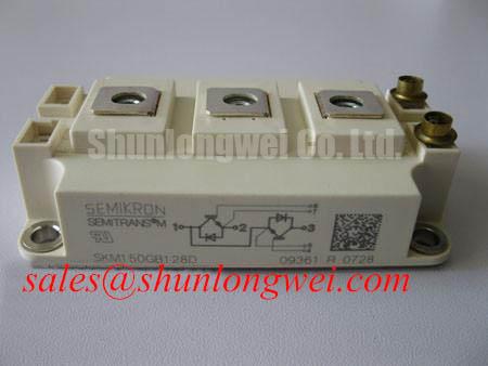
SEMITRANS is a Semikron-Danfoss module family; its SEMITRANS product information provides manufacturer context for the package family. Confirm model-specific dimensions, terminal assignments, and thermal data in the applicable SKM150GB063D documentation before changing mechanical or electrical interfaces.
Benchtop Gate Waveforms and High dv/dt Cross-Conduction
Probe gate-to-emitter voltage at the module connections while observing the corresponding switching-node waveform. A rising voltage across an off-state switch can couple through its reverse-transfer capacitance and disturb the gate. Whether that disturbance produces unintended conduction depends on the driver’s off-state impedance, wiring inductance, switching conditions, and the equipment’s protection sequence. Inspect both the commanded gate waveform and the off-state gate during controlled switching rather than inferring a fault from switching-node noise alone.
As an Engineering Recommendation, route gate-drive and return conductors close together and assess an active Miller clamp if the measured off-state waveform warrants it. Any negative gate bias must be checked against the module documentation and the driver’s limits; it is not a default setting for this product. 💡 Pro Tip: Keep the power-loop layout compact to limit turn-off overshoot, and confirm the voltage margin with a controlled double-pulse test.
When tracing a complete power stage, distinguish the SKM150GB063D switching position from surrounding devices on the schematic. A module such as SKM75GB07E3 can be examined as a separate topology reference, but its function and compatibility depend on the actual circuit, not its placement in a parts list.
Assembly Integrity and Transient Thermal Assessment
Before mounting, inspect the mating surfaces and confirm the heatsink pattern, terminal clearances, and fastening instructions against the original assembly documentation. Apply the specified interface material and mounting procedure for the equipment; uneven contact can make a calculated thermal margin unrepresentative of the installed module. After assembly, compare temperatures at repeatable measurement locations during a controlled load test and investigate changes in airflow or contact condition.
For pulsed overload evaluation, a steady-state heatsink reading does not establish peak junction temperature. As a Design Consideration, use the model-specific transient thermal impedance data and measured pulse sequence, if available, to estimate the junction response over successive pulses. Compare that estimate with the applicable manufacturer limits and allow for the starting temperature before each pulse. If the required thermal curve or limit is unavailable, do not substitute a generic multi-RC model as a claimed SKM150GB063D rating; obtain the relevant documentation before approving the duty cycle.