Content last revised on October 26, 2026
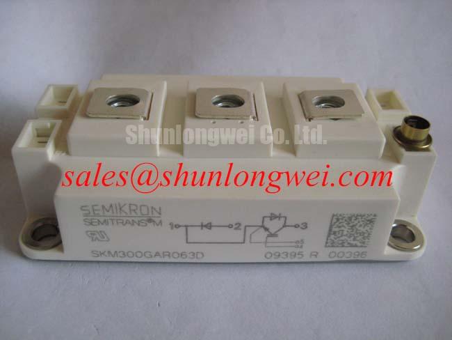
SKM300GB066D Semikron 600V 300A IGBT Module
With the inverter isolated, check the module terminals against the original wiring diagram, then record the cold-state diode response before applying gate-drive power. The SKM300GB066D is a Semikron IGBT Module with specified ratings of 600.0 V and 300.0 A, subject to the applicable datasheet conditions, and a Semitrans package designation.
For an incoming inspection bench, keep the device unpowered and protected against electrostatic discharge. Confirm terminal polarity from the equipment documentation, use the multimeter diode range only as a comparative screening method, and compare the reading pattern with a known-good module from the same circuit family. A diode-range result is not a substitute for a switching test or a manufacturer-defined semiconductor test curve.
| Parameter | Specification |
|---|---|
| Manufacturer | Semikron |
| Model | SKM300GB066D |
| Rated voltage | 600.0 V |
| Rated current | 300.0 A, subject to the applicable datasheet conditions |
| Package | Semitrans |
| Product category | IGBT Module |
💡 Bench Tip: Discharge the DC link, verify the absence of hazardous voltage, and remove gate-drive connections before cold-state checks, because stored energy or an active driver can distort diode measurements and expose the technician to hazardous voltage.
When evaluating a replacement for an industrial inverter welder or a medium-frequency induction-heating power supply, verify the original circuit topology, gate-driver reference, cooling arrangement, terminal layout, and protection network before installation. The Semikron-Danfoss SEMITRANS® Industry Standard IGBTs reference provides useful package-family context, while the actual electrical limits for this model must remain tied to its applicable technical documentation and system test results.
SKM300GB066D Operational Boundaries: Evaluating Commutation and Turn-Off Voltage Spikes
Turn-off evaluation should begin at the commutation loop, where stray inductance and gate timing influence voltage overshoot. If the installed circuit uses an antiparallel freewheeling diode, its reverse-recovery current can briefly add stress to the IGBT during the opposing device’s turn-on. A sharp recovery event can also increase electromagnetic emissions and ringing at the power terminals.
Use a properly rated differential probe at the relevant collector-emitter nodes and inspect the voltage waveform together with the gate-emitter signal. The useful comparison is between a stable reference waveform and the waveform produced after the module replacement. Look for excessive ringing, a delayed return to the DC-link level, or a gate disturbance that coincides with the commutation event. These observations help separate a gate-drive problem from a power-loop or snubber problem without assigning a single cause from one symptom.
RC snubber selection is a system-level damping task. The network should be evaluated against the measured ringing frequency, switching energy, capacitor pulse capability, resistor dissipation, and physical placement. Place the snubber loop close to the switching path it is intended to control, while keeping high-current and gate-control routing physically separated. Clearance around the high-voltage terminals should follow the equipment insulation design and applicable safety requirements rather than a generic spacing assumption.
When a turn-on edge produces a high reverse-recovery current, a slower external turn-on gate path may reduce the instantaneous commutation stress, but it can also increase switching loss. Designers should tune this tradeoff during controlled switching tests while checking peak voltage against the 600.0 V rating and the complete DC-link operating condition. The Semikron-Danfoss Power Electronics & Modules Official Hub offers broader manufacturer-level information on power module integration.
SKM300GB066D Thermal-Electrical Optimization: Practical Gate Drive Resistance Tuning
Retrofitting the SKM300GB066D into a legacy drive board requires separate attention to turn-on and turn-off gate resistance. The original driver may have been tuned for a different gate charge, switching speed, or module layout. Reusing the old resistor value without observing the gate waveform can produce an undesirable compromise between switching loss, voltage overshoot, and electromagnetic interference.
Start by confirming the gate-driver supply, isolation arrangement, gate-return path, and dead-time logic from the original equipment design. The gate signal should be measured directly at the module terminals, not only at the driver output, because the physical return path can introduce a difference between the commanded and actual gate-emitter voltage. If an auxiliary emitter or separate low-inductance return is present in the equipment design, route it independently from the high-current emitter path and verify that the module documentation supports that connection.
A larger turn-on resistance generally changes the rate at which channel current rises, while turn-off resistance affects the speed of current interruption and the resulting voltage excursion. These are design considerations, not fixed SKM300GB066D factory settings. Adjust one path at a time, observe collector-emitter voltage and gate-emitter behavior under the intended load, and check semiconductor temperature after the switching condition has stabilized.
Phase-angle conduction control and line-frequency ripple smoothing deserve separate review when the IGBT stage is connected to a rectifier front end. An uneven DC-link waveform changes the current stress seen during each switching interval and can make a gate setting appear acceptable at one line phase but unstable at another. Input filtering and control timing should be assessed for their effect on power-factor behavior and high-order line harmonics. The IGBT module itself should not be represented as independently providing system-level EMC compliance.
For an industrial inverter welder, inspect the output-current feedback and pulse timing while the gate resistance is being calibrated. For a medium-frequency induction-heating supply, pay particular attention to resonant-current transitions, because the switching waveform may change substantially with the work-coil load. The neutral option for a field replacement is to preserve the original protection architecture where it remains compatible, then validate the actual waveform and thermal response rather than selecting a resistor from a generic application table.
SKM300GB066D Operational Boundaries: Evaluating Transient Thermal Impedance Limits
Heavy pulsed overload must be assessed through the full heat path from junction to case, then from case to heatsink and cooling medium. A short current pulse can produce a different junction response from continuous operation, so the steady-state thermal resistance alone is not sufficient for evaluating repeated welding pulses or induction-heating bursts.
Use the applicable transient thermal impedance curve and represent the junction-to-case response with the manufacturer’s multi-section RC model when that information is available. In practical terms, each thermal section describes a time-dependent portion of the heat flow. Combine the calculated pulse loss with the case-temperature measurement and the actual duty sequence to estimate the junction-temperature margin. The calculation should use the real pulse width, repetition pattern, switching loss, conduction loss, and cooling condition established by the equipment test plan.
Thermal measurements become more useful when the mechanical interface is controlled. Clean the mating surfaces, apply a uniform and appropriately thin thermal interface layer, keep the module base flat against the heatsink, and tighten the mounting hardware in a controlled cross pattern according to the relevant mechanical documentation. Excess interface material can increase thermal resistance, while uneven pressure can distort the contact condition.
Do not infer thermal performance from the 300.0 A rating alone. Current capability depends on temperature, duty cycle, switching frequency, cooling, electrical waveform, and the module’s permitted operating area. During a retrofit, compare case temperature at equivalent load points and inspect whether the temperature rise follows the same pattern across repeated pulses. A sudden change in thermal behavior may justify checking mounting pressure, thermal-interface condition, switching loss, and current measurement accuracy together.
For engineering background on multilevel power-conversion arrangements and their efficiency tradeoffs, the Peak Efficiency in Solar and Energy Storage guide can be reviewed alongside the specific module documentation. It should be treated as system-level reference material rather than as a substitute for the SKM300GB066D thermal data.
SKM300GB066D Operational Boundaries: Evaluating Transmission Line Impedance Mismatch
Long motor leads and fast inverter edges can transform a manageable terminal transition into a reflected-wave problem. Cable impedance, motor input impedance, termination behavior, and switching rise time interact at the cable end. The resulting peak can appear at the motor terminals or return toward the module, so checking only the inverter-side waveform may miss the highest local stress.
For a variable-frequency drive using this 600 V module, measure the motor-side waveform with suitable high-voltage probing and compare it with the inverter terminal waveform. Inspect phase-to-phase and phase-to-ground behavior, cable routing, shield termination, and the physical distance between the power conductors and control wiring. A mismatch may present as ringing, repeated edge reflections, or a voltage pattern that changes when the cable length or motor is changed.
Output filters, dv/dt filters, and motor chokes should be selected from the complete drive and cable data, including current, switching frequency, insulation requirements, filter losses, and resonance behavior. Their purpose is to shape the voltage transition and limit stress at the motor terminals, but an unsuitable filter can introduce additional resonance or interfere with current control. The system engineer should verify the final waveform at both ends of the cable under the intended operating condition.
Maintain physical separation between high-energy commutation conductors, gate-drive wiring, sensing lines, and any auxiliary emitter return used by the drive architecture. Keep the power loop compact where possible, provide appropriate creepage and clearance for the working voltage, and avoid routing sensitive measurement conductors parallel to high-current switching paths over long distances. These layout measures support reliable troubleshooting of the SKM300GB066D in inverter-welder and induction-heating equipment without treating a general installation practice as a model-specific factory guarantee.
For a neutral replacement assessment, compare the existing mounting pattern, terminal markings, driver compatibility, cooling interface, and protection network before approving the change. A related Semikron device such as SKET400/08E may be evaluated separately where the circuit requirements call for that device class, but substitution decisions remain dependent on voltage, current, topology, gate-drive, thermal, and mechanical verification.