


Content last revised on September 20, 2026
Preventing Spurious Faults: Current Limit Mode vs Linear Voltage Ramp Guidelines for T9601612030H
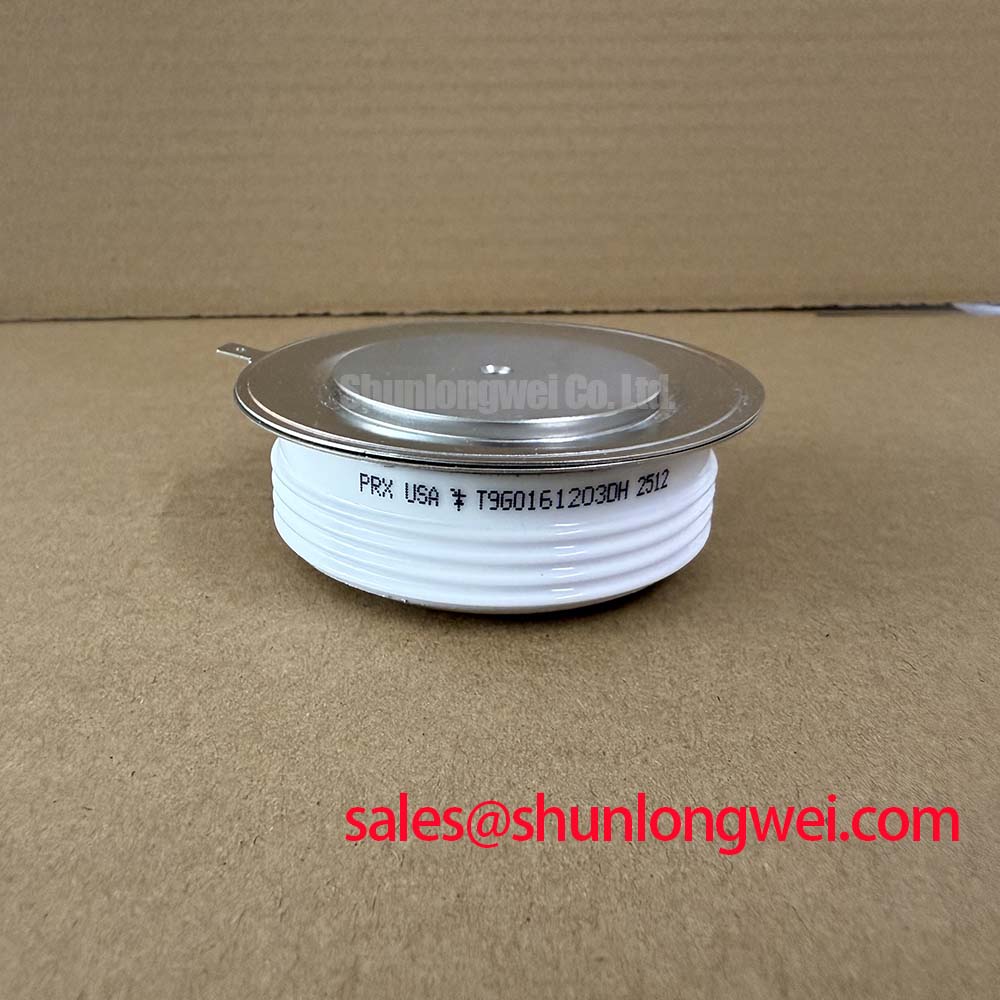
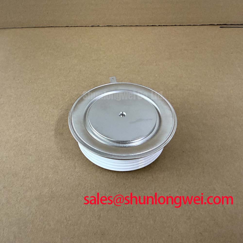
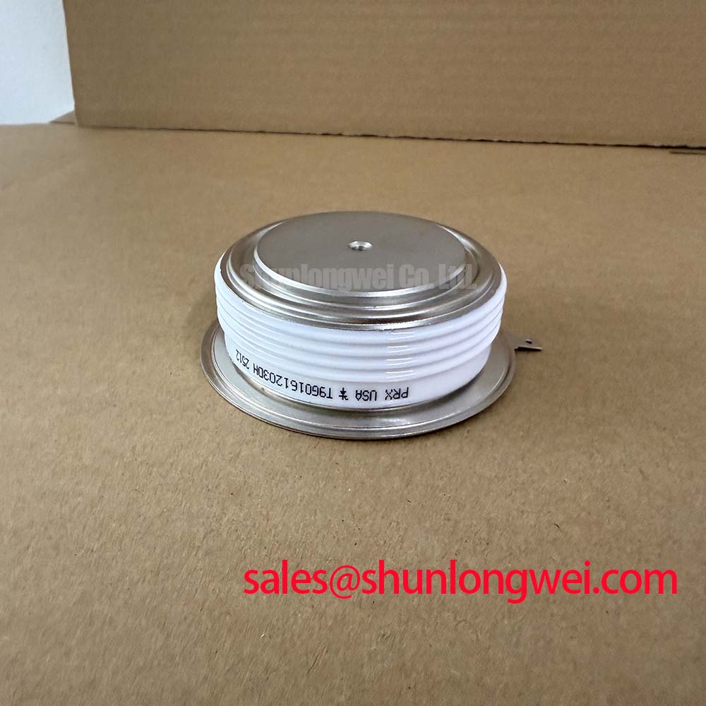
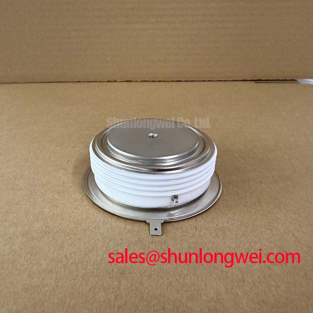
Before installation, isolate the assembly and compare each power terminal path against the original circuit drawing, then use a diode test function to check the gate-to-cathode junction and compare terminal behavior with a known-good module, without applying a gate trigger. The T9601612030H is a Powerex high current thyristor module rated at VDRM = 1600V and IT(AV) = 1200A under its official datasheet conditions. These ratings establish the electrical identity that should be checked before a replacement is fitted into a high voltage three phase motor solid state soft starter.
For soft starter service work, the controller strategy determines how the module is stressed during motor acceleration. A current limit mode usually regulates firing angle according to measured motor current, while a linear voltage ramp advances the firing point progressively over the programmed start interval. Both methods can be present in the same controller, but their behavior should be verified from the original control documentation and waveform capture rather than assumed from the module rating alone.
A locked rotor motor can draw several times its rated current. The purpose of a correctly commissioned current limit is to reduce that starting demand and avoid abrupt torque transfer through couplings, gearboxes, and driven machinery. In a power stage using the T9601612030H, the 1200A average forward current is an Official Datasheet Specification, not a guaranteed motor starting capability for every enclosure or duty cycle. The controller engineer should confirm the motor nameplate current, acceleration profile, bypass contactor sequence, phase balance, and the actual thermal state of the heatsink.
The module’s IT(RMS) rating of 1.88kA is especially useful when reviewing busbar and thermal paths. RMS current is relevant because phase controlled waveforms impose heating that is not described by average current alone. A soft starter that passes a short bench test may still develop uneven thermal loading if one phase fires late, one current transformer reports incorrectly, or one gate channel loses pulse continuity during the ramp.
| Official specification | Value | Integration relevance |
|---|---|---|
| Repetitive peak off state voltage | 1600V | Voltage boundary for the thyristor blocking state |
| Average forward current | 1200A | Rated average-current reference under specified conditions |
| RMS on state current | 1.88kA | Thermal review reference for conductors and heatsinking |
| Peak non repetitive surge current | 24.65kA | Fault and transient withstand reference |
| Maximum operating junction temperature | 125°C | Official thermal operating ceiling |
Fuse coordination must be reviewed using the fuse manufacturer’s time current and I²t data together with the original equipment protection design. The module’s 24.65kA peak non repetitive surge current is an Official Datasheet Specification, but it does not replace a coordinated semiconductor fuse. A protective device that clears too slowly can expose the device, buswork, and adjacent phase assemblies to energy beyond their intended limits.
T9601612030H Thermal Electrical Optimization: Preventing Localized Gate Hotspot Burnout Practical Tuning
Examine the gate and cathode control terminals for secure connection, insulation clearance, and correspondence with the original driver harness before energizing the main circuit. A thyristor gate is a trigger interface, and the available official information for the T9601612030H supplied here does not define gate trigger current, gate trigger voltage, pulse width, or permissible gate current rise time. Those values must be obtained from the applicable Powerex documentation or from the original equipment design records before a driver setting is changed.
Gate firing quality is best assessed with isolated oscilloscope measurements across each gate to cathode path while comparing all phases under the same controlled condition. A weak, delayed, interrupted, or incorrectly referenced pulse may contribute to unequal conduction and local heating, but waveform symptoms should not be assigned to one cause without checking the driver supply, trigger transformer or isolation circuit, control reference, and terminal condition.
Multi pulse firing is commonly used in phase controlled systems to preserve triggering while the device is forward biased. This is a Design Consideration, not an official operating requirement stated by the listed T9601612030H ratings. The system integrator should verify that pulse timing remains compatible with the motor control algorithm, phase voltage sensing, and the original board’s driver limits. Changing pulse repetition or pulse energy without confirming the gate specification can create a new failure mechanism rather than correct an existing one.
The stated 125°C maximum operating junction temperature is the official thermal ceiling. It should be treated as a boundary, not a normal target temperature. Thermal assessment should combine the actual start frequency, conduction angle, measured heatsink condition, airflow path, interface flatness, and measured phase current. The thermal expansion differences between materials can also affect clamping consistency across repeated thermal cycles. The general physical basis is described in this reference on thermal expansion coefficient mismatch in semiconductor assemblies.
💡 Bench Tip: Keep the gate drive disconnected during cold terminal checks, use ESD controlled handling, and compare the replacement module’s static readings with a known good phase before applying a firing signal.
For a thyristor soft starter, regenerative braking chopper operation and braking resistor energy absorption are normally separate system functions. They should not be attributed to the T9601612030H unless the equipment schematic explicitly places this module in that circuit. When reviewing a starter with a braking subsystem, technicians should trace the actual power topology and determine whether the component is used in the input phase control path, bypass path, or another defined branch.
Assembly Integrity & Layout Architecture: Minimizing Commutation Turn-Off Voltage Spikes for T9601612030H
Inspect the mounting faces, busbar contact surfaces, fasteners, and phase connections before tightening the module into the heatsink assembly. The official parameter set confirms high current capability, but it does not provide a manufacturer specified mounting torque, case dimensions, or terminal torque value. These mechanical values must therefore come from the original Powerex mechanical documentation and the equipment drawing rather than a generic torque chart.
The recommended service sequence is to remove oxidation, debris, old damaged interface material, and uneven residues from the heatsink surface, then confirm flat seating before final fastening. A thin and uniform thermal interface layer is a Design Consideration intended to avoid air gaps while preserving direct thermal contact. The system engineer should verify clamp load and interface condition against the approved assembly procedure.
Commutation behavior depends on the companion diode, line inductance, transformer leakage reactance, snubber network, cable routing, and firing angle. Reverse recovery peak current and recovery time are diode characteristics that should be reviewed from the actual diode data source. They are not published official ratings for the T9601612030H in the supplied specification set. If turn off transients appear excessive, measure phase voltage and current with suitable high voltage differential and current probes, then compare the result against a known good phase or approved commissioning trace.
Minimizing the physical commutation loop is an Engineering Recommendation for reducing inductive overshoot and radiated noise. The system design determines the acceptable conductor arrangement, snubber placement, and shielding approach. Verify peak voltage margins against the DC link or line voltage during controlled switching tests, rather than inferring safety from the 1600V blocking rating alone.
Where control circuits share a noisy reference with power connections, common mode ground movement can disturb firing signals. The equipment designer should preserve the original gate return routing and isolation arrangement. For broader background on gate turn off bias arrangements in power switching circuits, see Evolution of Negative Off Bias Gate Drive Circuits. This reference is informative; a negative gate bias must not be imposed on a thyristor gate circuit unless the original design documentation explicitly supports it.
T9601612030H Thermal Electrical Optimization: Critical Rate of Rise of Off State Voltage Practical Tuning
With the main power section isolated, check the RC snubber capacitors, resistors, wiring continuity, and terminal insulation before attributing nuisance firing to the thyristor module. A damaged snubber, loose connection, incorrect phase reference, or external transient may affect off state behavior. The supplied official data identifies VDRM = 1600V, but it does not state a critical rate of rise of off state voltage, an RC snubber value, or a series reactor requirement for this exact part number.
RC snubber sizing is therefore a system level Design Consideration. Its purpose is generally to moderate voltage rate of rise and transient stress across a blocking semiconductor. The appropriate resistance, capacitance, capacitor pulse capability, and resistor energy rating depend on the line voltage, transformer characteristics, cable length, load behavior, measured transient waveform, and existing control arrangement. Any revision should be validated through controlled tests by the responsible system engineer.
Series saturable reactors are also application dependent. They can influence current rise and commutation behavior, but their selection cannot be derived from the T9601612030H’s current and voltage ratings alone. Before changing reactor hardware, confirm the original phase assembly, bypass contactor timing, fuse coordination, and current sensing response. An incorrect modification can alter starting torque, increase thermal stress, or produce phase imbalance.
For practical incoming inspection, record cold state terminal behavior, compare phase assemblies, verify insulation spacing, and retain oscilloscope captures from the first controlled firing test. The 1600V blocking rating, 1200A average current rating, 1.88kA RMS current rating, 24.65kA surge current rating, and 125°C maximum junction temperature provide the correct official boundaries for evaluating the T9601612030H within a documented high voltage motor soft starter design.