
Content last revised on September 20, 2026
Assembly Integrity & Layout Architecture: Implementing Phase Controlled Rectification and Firing Angle Control for TT104N14KOF
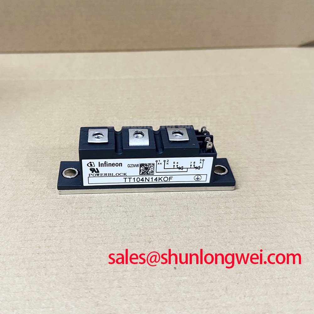
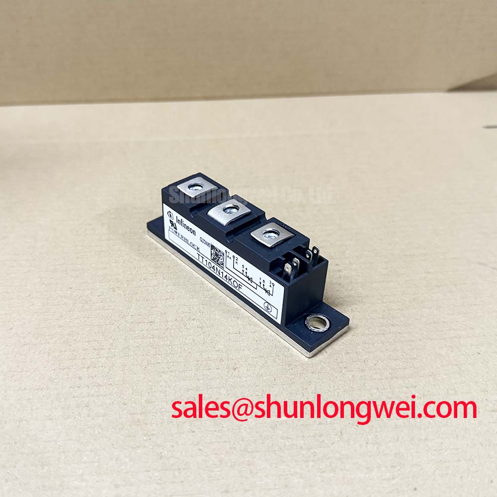
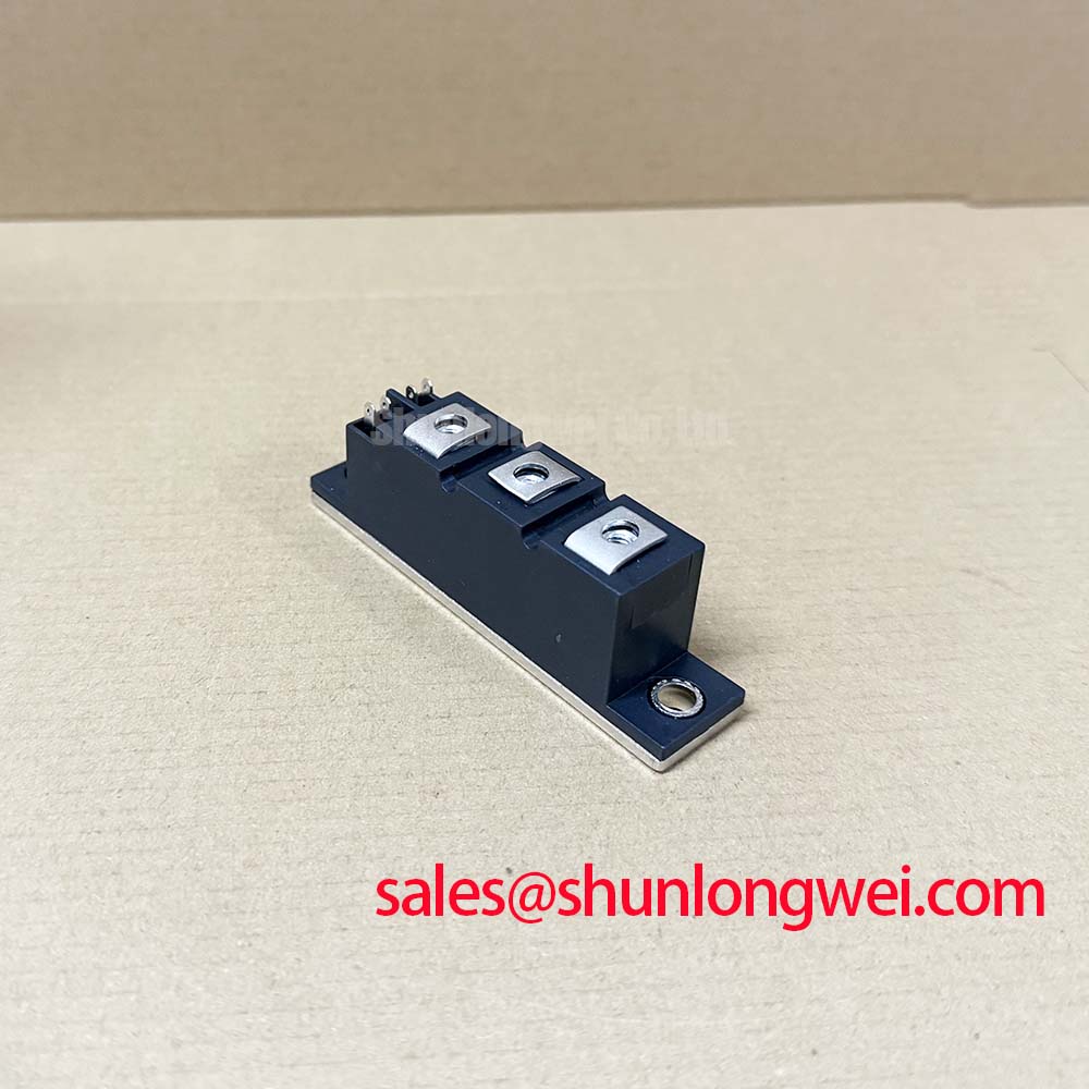
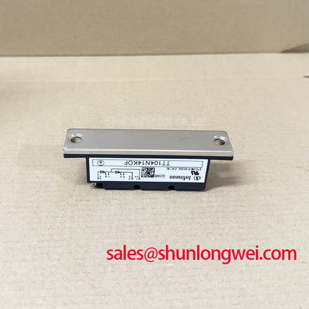
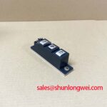
For phase controlled rectifier assemblies, confirm that the thyristor connections follow the original bridge or anti parallel circuit drawing before reconnecting gate leads. The TT104N14KOF is a dual thyristor module, so its electrical role depends on the surrounding topology rather than on the module alone. In a controlled AC to DC supply, the firing angle determines when each thyristor begins conduction within the AC waveform. A lower firing angle generally transfers more rectified energy to the load, while a later firing angle reduces average DC output and increases reactive demand on the upstream supply.
For medium frequency induction melting and hardening furnace power supplies, the rectifier firing sequence should be checked against the original controller timing, line synchronization reference, and transformer phase relationship. Designers should verify current waveform distortion, input power factor, and transformer heating under the actual firing angle range rather than assuming that a module voltage rating alone establishes system suitability.
| Official Datasheet Specification | Condition | Value |
|---|---|---|
| Repetitive peak off state voltage | VDRM, VRRM | 1400 V |
| Average on state current | TC = 85°C | 104 A |
| RMS on state current | TC = 55°C | 200 A |
| Surge current | 10 ms, Tvj = 25°C | 1900 A |
| Isolation voltage | RMS, 50 Hz | 3600 V |
| Terminal torque | Official specification | 5 Nm |
Fuse selection requires coordination with the actual prospective fault current, conductor withstand capability, and the fuse manufacturer’s published clearing characteristics. The supplied module data identifies a 1900 A surge-current condition, but it does not provide a module fuse I²t coordination value. Therefore, fuse I²t matching remains a system level Design Consideration requiring the fuse data sheet and equipment fault study.
⚠️ Maintenance Note: Recheck terminal tightness to the official 5 Nm specification during planned shutdowns, and monitor contact temperature rise while confirming that cooling air paths remain clear.
TT104N14KOF Circuit Protection & Reliability: Calibrating AC Line Surge Immunity and Lightning Transients
The 1400 V repetitive off state rating is an Official Datasheet Specification, not a complete AC line transient protection plan. Input surge protection should be evaluated at the complete assembly level, including incoming feeder impedance, transformer coupling, contactor switching behavior, and the voltage appearing at the thyristor terminals. MOV and RC protection networks are Design Considerations that require verification against the equipment’s measured surge waveform and the selected protection component ratings.
Where the installation specification references IEC 61000 4 5 surge testing, the test level, source impedance, and coupling arrangement should be established by the system designer. A thyristor module cannot by itself be represented as compliant with equipment level EMC or surge standards. Place protective elements so that the conductor path between the protected node and the module is controlled, because excessive loop area can reduce the practical benefit of a clamp or snubber.
In high energy rectifier cabinets, inspect thermal interfaces whenever the module is removed. The maximum junction to case thermal resistance is 0.25 K/W per thyristor, according to the official specification. Heat sink flatness, thermal compound condition, airflow, and ambient moisture control remain Design Considerations that influence the temperature difference between junction and case during real load cycles.
For a related high current thyristor position in a shared conversion platform, engineers can compare the published electrical boundaries of TT500N18KOF without treating it as an automatic substitute. Voltage class, firing circuit capability, thermal interface, and physical installation details must be reviewed against the original equipment documentation.
TT104N14KOF Operational Boundaries: Evaluating Critical Rate of Rise of Off State Voltage Limits
A thyristor exposed to a fast rising off state voltage can be susceptible to unintended triggering if the complete circuit creates sufficient displacement current through its internal junction capacitances. The official parameter set provided for TT104N14KOF does not specify a critical off state voltage rate of rise. Engineers should therefore avoid assigning an unsupported numerical dv/dt limit and should validate the module terminal waveform with suitable high voltage measurement methods during switching tests.
RC snubbers and series saturable reactors are system dependent Design Considerations. Their purpose is to moderate the rate at which voltage and current change during commutation, particularly where transformer leakage inductance and busbar geometry create transient stress. Component values should be selected through measured waveforms, power dissipation review, and validation of peak terminal voltage relative to the 1400 V official repetitive rating.
Keep the power path compact and maintain a consistent connection arrangement between parallel rectifier legs. This reduces unequal parasitic impedance that can alter commutation behavior. If a repair requires a different current class, TT570N16 can be reviewed as a separate technical reference, subject to a full check of circuit topology, mechanical fit, cooling capacity, and gate trigger requirements.
Preventing Spurious Faults: Gate Trigger Current and Temperature Dependent Guidelines for TT104N14KOF
The TT104N14KOF has a maximum gate trigger current of 150 mA at Tvj = 25°C. This is an Official Datasheet Specification that defines a key firing interface boundary, but it does not establish the required gate drive pulse waveform for every converter. Gate driver output capability, isolation arrangement, gate lead routing, and noise coupling should be assessed against the existing firing board and the module documentation.
In phase controlled systems, a firing pulse that is poorly synchronized, insufficiently sustained, or disturbed by common mode noise may produce irregular conduction. This does not confirm a single cause. Check the synchronization signal, gate to cathode waveform, polarity, repeated firing strategy, and supply stability against a known good channel where available. The system integrator should verify pulse rise behavior and pulse duration across the applicable temperature range rather than relying on room temperature observations alone.
Gate wiring should be separated from high current AC and DC power conductors where practical, while return paths should remain intentional and low impedance. For general gate drive architecture and isolation interface context, see the Infineon Gate Driver ICs Portfolio. The referenced portfolio is a general technical resource and does not replace TT104N14KOF thyristor firing verification.
Long term preventive maintenance should include cleaning heat sink fins, checking fan operation, reviewing thermal compound condition, and preventing condensation around gate and power terminals. Teams evaluating gate turn off bias concepts in other controlled power stages may also consult Evolution of Negative Off Bias Gate Drive Circuits. That discussion is useful for broader drive circuit assessment and should not be interpreted as a prescribed bias requirement for this thyristor module. For IGBT module packaging context, the Infineon TRENCHSTOP™ 5 technical article describes a separate IGBT technology family and is not a source of TT104N14KOF ratings.