Content last revised on September 14, 2026
TT500N18KOF Circuit Protection & Reliability: Ensuring Uniform Heatsink Contact Pressure
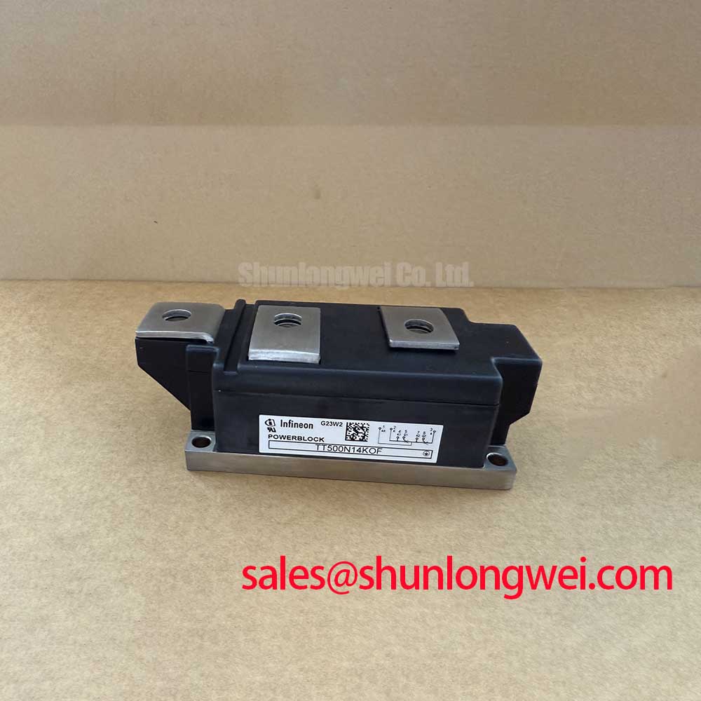
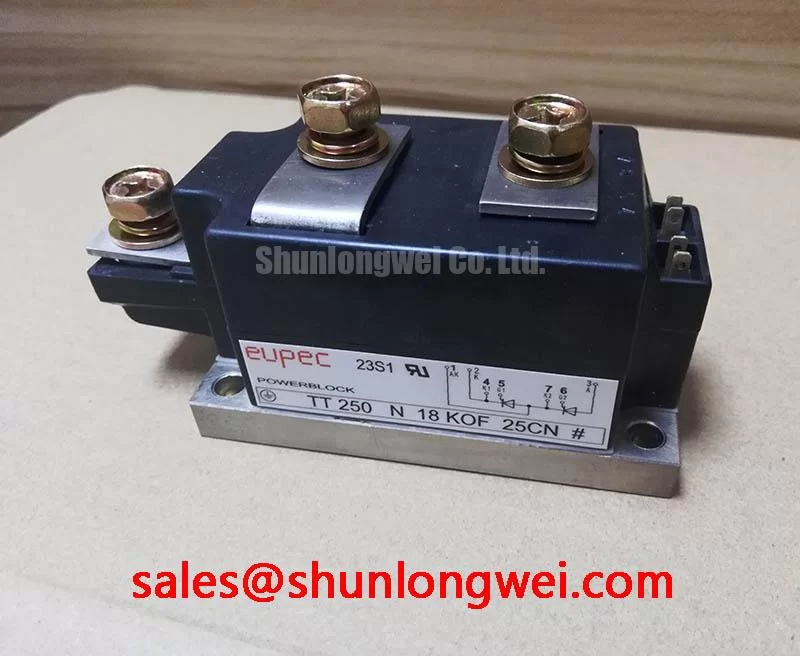
With the unit isolated from all energy sources, begin incoming inspection by comparing the terminal arrangement with the original equipment documentation and performing preliminary diode-mode checks on each thyristor path at room temperature. The TT500N18KOF is an Infineon dual thyristor module with an official repetitive peak off state and reverse voltage rating of 1800 V. Its official average on state current rating is 500 A at TC = 85°C, making correct terminal identification, clean contact faces, and controlled clamping pressure essential before it is returned to service.
The published DC junction to case thermal resistance is 0.055 K/W. This is an Official Datasheet Specification for the thermal path from the semiconductor junction to the module case, not a guarantee of complete assembly thermal performance. The installed result also depends on heatsink flatness, cleanliness, thermal interface material coverage, fastening sequence, and whether the mounting surface creates balanced pressure across the baseplate.
Before applying thermal compound, inspect the heatsink for embedded debris, raised burrs, corrosion, or local damage. Apply the interface material as a thin continuous film sufficient to fill surface irregularities, without allowing excess material to contaminate terminals or insulation areas. Tighten mounting hardware progressively in an alternating pattern so the module settles evenly. Mounting torque is a Design Consideration: the correct value must be verified against the module datasheet mounting instructions, screw size, heatsink construction, and equipment manufacturer requirements rather than inferred from another package family.
💡 Bench Tip: Record cold diode mode readings and terminal to case isolation checks before mounting, then compare them with the same readings after clamping to catch an installation related anomaly before energization.
The 2500 V RMS isolation voltage for 50 Hz over one minute is an Official Datasheet Specification. It supports a defined dielectric test condition, but it does not replace a full system review of creepage, enclosure contamination, cable routing, and transient protection. In assemblies exposed to line borne overvoltage, an MOV network can be evaluated as a system level suppression measure. The system engineer should verify its clamp behaviour, energy capability, and coordination with the actual supply and switching transient waveform.
For context on power device portfolios and package approaches, see Infineon’s OptiMOS™ and CoolMOS™ power semiconductor information and its EconoPACK™ Plus module range. These resources describe different power semiconductor categories and should not be treated as specifications for the TT500N18KOF.
Field Diagnostics & Commissioning: Evaluating Post Surge Reverse Voltage Blocking in TT500N18KOF Topologies
After a surge event, do not immediately restore the reverse blocking condition. The TT500N18KOF has an official non repetitive surge on state current rating of 14500 A for 10 ms at Tvj max, with 17000 A at 25°C. These values describe defined short duration conditions and must not be interpreted as recurring operating current capability.
Allow the assembly to return to a safe, controlled test state, then inspect external bus joints, fuse connections, snubber parts, and the contact condition of the module terminals. Measure the thyristor paths using the same meter, leads, polarity, and ambient conditions used for the pre service baseline. A changed reading can indicate the need for additional investigation, while an unchanged cold reading alone cannot prove dynamic blocking performance. Controlled equipment level testing should verify that the re applied voltage remains within the 1800 V official repetitive blocking limit.
The module’s official maximum RMS on state current is 900 A. During commissioning, engineers should compare measured phase current, heat sink temperature trend, and firing behaviour with the original converter control records. In grid tied static var compensator and thyristor switched capacitor equipment, transient response can also involve reactor, capacitor bank, busbar, and control timing conditions. A fault should therefore be isolated through measurements rather than assigned to the module from a single symptom.
For broader test concepts involving blocking conditions, current paths, and semiconductor protection, technicians can consult The Ultimate IGBT Knowledge Base as a general power semiconductor reference.
Field Diagnostics & Commissioning: Dynamic Firing Delay Angle Adjustment in TT500N18KOF Topologies
In phase controlled AC to DC sections, changing the firing delay angle from 0° toward 150° changes the conduction interval and the average converter output. It also changes input current shape, displacement behaviour, and reactive power demand. This is a system transfer characteristic, not an individual TT500N18KOF factory setting.
When recommissioning a controlled rectifier or capacitor switching branch, verify gate pulse presence and timing at the original test points with suitable isolated instrumentation. Compare the measured phase relationships against the controller’s approved timing references before permitting higher energy operation. Uneven firing can be associated with gate drive issues, synchronisation loss, external connection resistance, or power circuit conditions, so each path needs examination.
The on state model values of 0.85 V threshold voltage and 0.35 mΩ slope resistance at maximum junction temperature are Official Datasheet Specifications. They help describe conduction behaviour at the stated temperature condition, but they are not substitute values for a complete converter loss calculation. Designers should assess actual current waveform, duty, cooling condition, and firing angle in the installed system.
Where a related phase controlled device is being assessed within the same equipment topology, the TD210N12 can be reviewed as a separate component reference. Electrical ratings, mechanical arrangement, trigger requirements, and protection coordination must be verified independently before any service decision.
Preventing Spurious Faults: I2t Sub Cycle Melting Rating Guidelines for TT500N18KOF
The official TT500N18KOF I²t rating is 1051 kA²s for 10 ms at Tvj max. This value provides a defined semiconductor withstand reference for fault coordination. It should not be treated as a universal fuse selection value or as proof that a particular protection assembly will prevent mechanical damage under every fault condition.
Fuse coordination requires review of the prospective fault current, fault duration, semiconductor fuse pre arcing characteristic, total clearing characteristic, cable contribution, and the actual location of the fault. The protection objective is to limit energy let through before the semiconductor’s specified short duration withstand capability is exceeded. This is an Engineering Recommendation requiring the original system fault study and verified manufacturer curves.
Check that fuse holders and terminal joints are secure, clean, and sized according to the equipment documentation. Loose connections can add heat and create misleading voltage drop observations during loading. If a higher current alternative is being evaluated strictly for comparison, the TT570N16 should be assessed only through its own datasheet ratings, package requirements, protection coordination, and installed circuit conditions.