Content last revised on August 28, 2026
Cosmic Ray Robustness: Voltage Derating Curves across 2000m-4000m Altitudes
Heavy-duty variable frequency AC motor drives installed in high-altitude environments face accelerated failure rates due to atmospheric terrestrial neutron flux. At altitudes between 2000m and 4000m, the cosmic-ray-induced Single Event Burnout (SEB) rate increases exponentially compared to sea-level operations. For the 1MBI200NH-060, which possesses an absolute maximum collector-emitter rating of VCES = 600V, managing the DC-bus voltage headroom is essential to maintaining acceptable Failure In Time (FIT) metrics.
High-energy neutrons colliding with the silicon lattice generate localized charge carriers that can trigger catastrophic avalanche breakdown when the applied electric field exceeds critical limits. To suppress SEB failure rates in high-altitude industrial drive topologies, the operating DC-link voltage must be derated relative to the rated 600V maximum. For detailed failure physics and standard accelerated testing protocols under severe conditions, consult the Field Engineer’s Handbook. In high-voltage installations where derating 600V modules compromises the operational DC-bus window, systems requiring higher voltage headroom may integrate 1200V-class single modules such as the 1MBI200SA-120B.
High-Frequency Commutation Loop Inductance Minimization in High-Power Arrays
In heavy-duty inverter power stages switching continuous DC currents of IC = 200A (at Tc = 25°C) and peak currents of ICP = 400A (1 ms pulse), the turn-off di/dt creates substantial overvoltage transients. The collector-emitter voltage spike is governed by the relation:
Vpeak = VDC + Lsigma · (di/dt)
To prevent Vpeak from exceeding the 600V breakdown threshold during hard turn-off events, the total stray inductance of the commutation loop (Lsigma) must be strictly constrained below 25nH. Achieving this requirement demands laminated planar busbar architectures where the forward and return current paths are closely coupled to cancel mutual magnetic flux.
Mounting integrity directly influences both loop inductance and thermal dissipation. The 1MBI200NH-060 requires a mounting torque of 3.5 N·m (M5 screws) for both heatsink attachment (Ms) and main power terminal connections (Mt). Maintaining this specified torque ensures stable mechanical contact, minimizes junction-to-case thermal resistance Rth(j-c), and prevents contact interface degradation under high-vibration heavy-duty motor duty cycles. Standard construction guidelines for advanced industrial modules are documented via the Fuji Electric RC-IGBT Modules technical library and the broader Fuji Electric Power Semiconductors Portal.
Dynamic Gate Impedance Control for Robust Phase-Leg Dead-Time Operation
In bridge converter topologies, high dv/dt transients during phase-leg switching generate displacement currents through the collector-gate Miller capacitance (Cres). This current flows into the gate driver circuit according to:
iMiller = Cres · (dv/dt)
If this dynamic current creates a voltage drop across the gate turn-off resistance that exceeds the gate-emitter threshold voltage VGE(th) (specified between 5.5V and 8.5V at VCE = 20V, IC = 200mA), parasitic shoot-through occurs across the DC bus. The saturation performance of the module exhibits a maximum VCE(sat) = 2.7V at VGE = 15V and IC = 200A, which requires stable positive drive voltage for low conduction loss and dedicated dynamic gate management to prevent false turn-on.
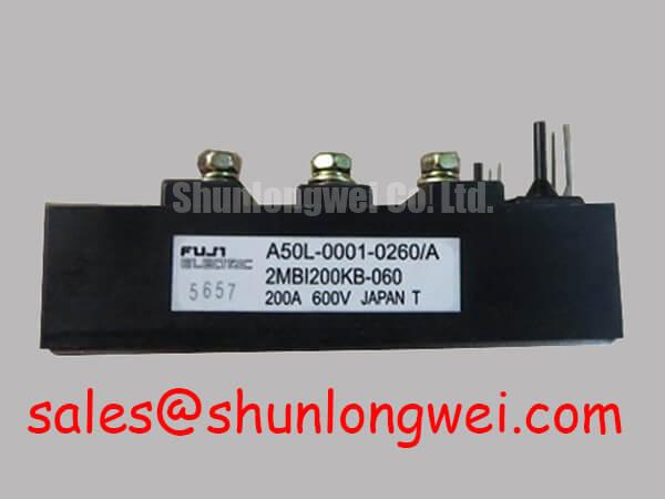
Mitigation strategies involve deploying negative gate bias voltages (-5V to -15V) during the turn-off phase, or implementing active Miller clamping circuits. When selecting topologies for half-bridge assemblies, discrete single-switch configurations may be evaluated alongside half-bridge modules; for dual-switch requirements within the same current rating, the 2MBI200KB-060 provides an integrated two-pack alternative.
PCB Gate Loop Layout Symmetry & Kelvin Emitter Routing Optimization
Parasitic emitter inductance shared between the main power loop and the gate drive loop introduces negative feedback that slows switching transitions and increases turn-off losses (Eoff). The 1MBI200NH-060 provides dedicated auxiliary terminals to establish a true Kelvin emitter connection, isolating the gate drive return path from the high di/dt power loop carrying up to 400A pulsed current.
The PCB layout must maintain tight physical symmetry between forward gate traces and return Kelvin emitter traces to reduce effective loop area, thereby minimizing electromagnetic susceptibility to radiated phase currents. Operating across a broad junction temperature range of Tj = -40°C to +150°C with an isolation voltage rating of Viso = 2500V AC (1 min), the internal insulation system maintains electrical barrier integrity while optimized gate routing prevents high-frequency ringing and gate-oxide dielectric breakdown during fast switching transients.
Summary Technical Specifications
| Parameter | Symbol | Rated Value / Test Condition | Unit |
|---|---|---|---|
| Collector-Emitter Voltage | VCES | 600 | V |
| Continuous DC Collector Current | IC | 200 (Tc = 25°C) | A |
| Pulsed Collector Current | ICP | 400 (1 ms) | A |
| Gate-Emitter Threshold Voltage | VGE(th) | 5.5 – 8.5 (VCE = 20V, IC = 200mA) | V |
| Collector-Emitter Saturation Voltage | VCE(sat) | 2.7 (Max, VGE = 15V, IC = 200A) | V |
| Isolation Voltage | Viso | 2500 (AC 1 min) | V |
| Operating Junction Temperature | Tj | -40 to +150 | °C |
| Mounting Screw Torque | Ms / Mt | 3.5 (M5 screws) | N·m |