
Content last revised on September 10, 2026
Baseplate Convexity Compensation and Screw Tightening Sequence Guidelines
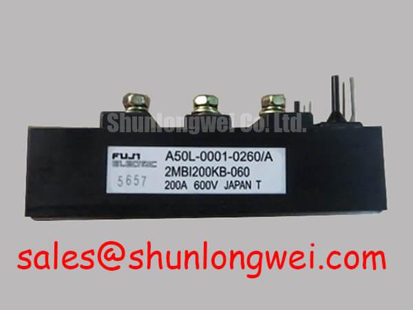
In incoming quality assurance and bench validation, mechanical flatness is a primary screening metric for the 2MBI200KB-060 dual IGBT module. Power cycling reliability in 1500V multi-string solar inverters directly correlates with the interface pressure profile between the module's copper baseplate and the extruded aluminum heatsink. Factory specifications define a technical baseline with continuous collector current IC = 200A, VCES = 600V, and an isolation withstand voltage Viso = 2500V AC for 1 minute.
Because the copper baseplate features a built-in pre-convexity (typically +20 to +80 µm) designed to flatten under thermal compression, improper torque application creates asymmetric voiding in the thermal interface material (TIM). When applying non-curing thermal grease, target a uniform wet film thickness between 50 µm and 100 µm using a calibrated screen printer or steel roller. Excess grease increases conductive thermal resistance, whereas insufficient thickness causes air entrapment, accelerating localized thermal runaway under Tj(max) = 150°C junction limits.
| Parameter Symbol | Technical Specification | Bench Verification Condition | Factory Limit |
|---|---|---|---|
| VCES | Collector-Emitter Voltage | VGE = 0V, IC = 1.0mA, Tj = 25°C | 600V min |
| IC / ICP | Continuous / Peak Current | DC / 1ms Pulse Width limit | 200A / 400A max |
| VCE(sat) (terminal) | Collector Saturation Voltage | IC = 200A, VGE = 15V, Tj = 25°C | 1.85V (typ) / 2.2V (max) |
| VF | FWD Diode Forward Drop | IF = 200A, VGE = 0V, Tj = 25°C | 2.0V (typ) / 2.4V (max) |
⚠️ Field Alert: Never torque mounting screws to full specification in a single step. Tighten mounting screws (M5) across the diagonal pattern to a provisional torque of 0.5 N·m to allow TIM redistribution. After a 10-minute relaxation pause, apply the final operational torque of 2.5 to 3.5 N·m. Unequal mechanical stress will deform the internal direct bonded copper (DBC) ceramic substrate, causing micro-fractures under repetitive diurnal thermal cycles.
SCSOA Overcurrent Protection: Implementing Two-Step Gate Voltage Clamping
The Short Circuit Safe Operating Area (SCSOA) of the 2MBI200KB-060 dictates that fault conditions must be fully cleared within 10 µs at nominal DC-link operating levels. In high-power inverter topologies, short-circuit events fall into Type-I (fault established before turn-on) and Type-II (hard short occurring while conducting). During hard de-saturation, the collector current spikes beyond 4 to 6 times the rated IC (200A), pulling the collector-emitter voltage out of saturation.
Abruptly pulling the gate voltage to 0V or negative potential under peak short-circuit currents creates a catastrophic rate of current change (di/dt). Across the parasitic stray inductance (Lσ) of the DC busbar and module terminals, this generates a severe overvoltage transient governed by:
ΔVCE = Lσ × (di/dt)
To keep the total instantaneous voltage safely below the VCES = 600V breakdown threshold, gate driver circuits must integrate a two-step soft turn-off (2SSTO) sequence. Upon desaturation detection via a high-voltage sensing diode, the gate voltage is clamped down from +15V to an intermediate level (+7V to +8V) for 2 to 4 µs. This reduces the di/dt slope before the final negative off-state bias drops the gate below the threshold, suppressing the inductive turn-off voltage peak. Complementary topologies in peripheral chopper paths often deploy discrete devices such as the 1MBI200NH-060, which requires matched soft turn-off timing to prevent cross-tier voltage breakdown.
Symmetrical Busbar Geometry for High-Current Parallel Module Arrays
Utility-scale solar inverters frequently combine half-bridge modules in parallel to expand output current. Paralleling the 2MBI200KB-060 requires balanced dynamic and static current sharing. In static conduction, the module exhibits a positive temperature coefficient in its terminal saturation voltage at elevated temperatures (shifting from VCE(sat) 1.85V typical at 25°C to higher levels at 125°C). This positive coefficient naturally promotes static thermal balance by shifting current away from hotter dies.
Dynamic current sharing during switching transients depends on physical layout symmetry rather than silicon parameters. Asymmetrical busbar geometry creates unbalanced stray loop inductances. A variance as small as 5 nH between parallel branches results in unequal di/dt distributions, causing one module to absorb excess turn-on and turn-off energy. Implement planar, laminated busbars with positive and negative conductors placed in close proximity to maximize mutual magnetic cancellation.
💡 Bench Tip: During incoming bench testing, measure gate threshold voltage VGE(th) across batches at IC = 200mA and VCE = 10V. Modules grouped within the same parallel leg should have a VGE(th) spread within ±0.2V. For applications requiring higher DC-bus margins or 1200V ratings in higher input voltage strings, engineers evaluate modules such as the 2MBI200SB-120 to maintain operating headroom.
Negative Gate Bias vs Active Miller Clamping in Fast-Switching Half-Bridges
The high dv/dt generated across the phase leg during transition states poses a continuous risk of cross-conduction shoot-through. When the upper IGBT turns on at high switching speeds, the rising voltage edge applies a high displacement current across the collector-gate Miller capacitance (Cres / Cgc) of the lower IGBT:
iMiller = Cres × (dv/dt)
This displacement current flows through the internal gate series resistance and external gate drive loop, raising the gate-emitter potential. If this voltage exceeds the internal turn-on threshold (typically VGE(th) = 5.5V to 7.5V), parasitic shoot-through occurs, inducing high thermal losses and potential module destruction. To mitigate this effect, power stage designs implement two complementary solutions:
- Negative Gate Off-State Bias: Applying a reverse gate bias of -5V to -15V (within the absolute maximum rating of VGES = ±20V) widens the noise margin, ensuring the gate stays well below threshold despite displacement spikes.
- Active Miller Clamping (AMC): An integrated driver circuit monitors the gate potential during turn-off. When the gate falls below +2.0V, a low-impedance auxiliary MOSFET directly shorts the gate terminal to the negative supply rail, bypassing external gate resistors and sinking the Miller current safely.
Detailed evaluation protocols, ESD protection procedures, and test setups for validating module health under static and dynamic bench scenarios can be explored in the Field Engineer’s Handbook. Engineers seeking structural architecture insights across newer-generation platforms can consult the Fuji Electric 7th-Gen X-Series IGBT Modules technical documentation, or review dedicated dynamic braking configurations in the Fuji Electric Brake Chopper IGBT Modules portfolio to coordinate drive stage timings.