Content last revised on September 10, 2026
Junction-to-Heatsink Heat Dissipation in High-Duty Industrial Phase Modules
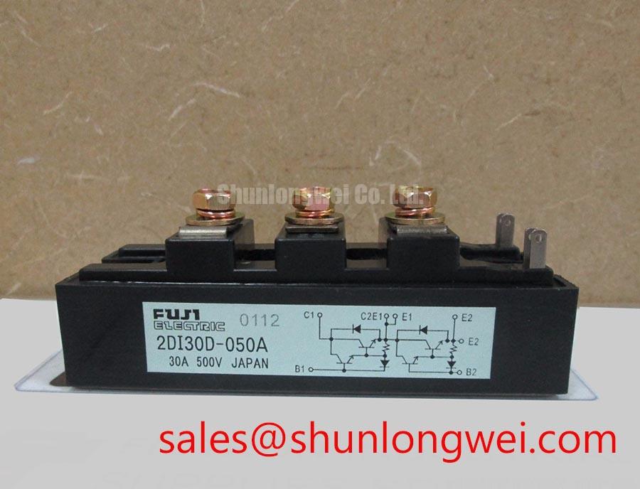
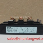
In medium-frequency induction melting and hardening furnaces, power semiconductor stages endure continuous thermal pulsing under fluctuating load impedances. The Fuji Electric 2DI30D-050A dual power Darlington/diode module is rated for a continuous collector current (IC) of 30A and a maximum collector power dissipation (PC) of 250W, with an allowable internal operating junction temperature (Tj) spanning -40 to +150°C. Managing this heat envelope requires strict attention to the thermal interface between the module copper baseplate and the system heatsink.
Thermal impedance mismatch or uneven mounting pressure leads to localized thermal runaway during high-duty induction cycles. Engineers must ensure the mounting surface maintains a flatness within 50 μm and a surface roughness under 1.6 μm. Applying a uniform thermal interface material (TIM) layer of 60 to 80 μm prevents dry spots without causing thermal grease migration under thermal cycling. Uniform screw torque distribution is mandatory; M5 mounting screws should be torqued progressively to 1.5–2.0 N·m in a diagonal pattern. For thermal validation protocols and transient thermal impedance analysis in industrial machinery, consult the Field Engineer’s Handbook.
Reverse Recovery Charge Temperature Coefficient and Dynamic Snubber Energy Dumping
Induction heating inverters operate with rapid commutations where free-wheeling diode recovery characteristics dictate turn-on switching stress. The internal antiparallel diodes in the 2DI30D-050A feature optimized dynamic behavior, yet reverse recovery peak current (Irrm) and recovery time (trr) exhibit positive temperature coefficients. At junction temperatures approaching 125°C, reverse recovery charge increases, elevating dynamic switching losses and generating high dv/dt transients.
To keep off-state voltage spikes well within the collector-emitter voltage limit (VCEO) of 600V, power stages require balanced snubber topologies. Metal oxide varistors (MOVs) paired with low-inductance ceramic snubber capacitors absorb inductive kickback energy from stray busbar inductance. Precise device characterization and thermal parameters are detailed directly on the Fuji Electric Power Semiconductors Portal to assist hardware designers during snubber network dimensioning.
Fuse Total Clearing I2t versus Device Melting Integral across 10ms Conduction Margins
Short-circuit conditions in metal hardening power converters—caused by coil flashovers or workpiece contact—require rapid fault clearing before the semiconductor package ruptures. Protecting the 2DI30D-050A requires strict coordination between the semiconductor protection fuse total clearing I2t and the module melting integral under a 10ms half-sine surge envelope.
| Parameter | Symbol | Datasheet Rating | Application Design Margin |
|---|---|---|---|
| Collector-Emitter Voltage | VCEO | 600V | Operate ≤ 480V DC Bus under dynamic surge |
| Continuous Collector Current | IC | 30A | Derate to 20–24A at heatsink Tc = 80°C |
| Maximum Collector Dissipation | PC | 250W | Maintain heatsink Rth(s-a) ≤ 0.35 K/W |
| DC Current Gain (Min) | hFE | 100 | Drive with IB ≥ 0.3A for deep saturation |
| Emitter-Base Voltage Limit | VEBO | 7V | Clamp reverse base drive to ≤ 5V |
High-speed current feedback loops utilizing isolated Hall Effect Sensors for Industrial Current Measurement provide sub-microsecond trip signals to the control unit, preventing repetitive surge degradation. When retrofitting legacy induction power cabinets or expanding to higher voltage designs, field service teams also evaluate higher-rated modules such as the 2DI50A-140 for systems operating at elevated voltage thresholds.
Preventing Localized Gate Hotspot Burnout via Fast-Rise Auxiliary Trigger Circuits
Darlington configurations demand adequate forward base current drive to minimize saturation voltage VCE(sat) and prevent current crowding across the input transistor junction. With a minimum DC current gain (hFE) of 100, the 2DI30D-050A requires a steep base current pulse (diB/dt > 1A/μs) at turn-on to achieve uniform emitter conduction and avoid localized hotspot burnout.
Engineers must respect the emitter-base voltage limit (VEBO) of 7V. Applying excessive negative base bias during turn-off can trigger avalanche breakdown of the input base-emitter junction, degrading current gain over time. The auxiliary base and emitter terminals must be routed using tightly twisted pairs directly to the driver board to isolate the gate drive loop from the high-current commutation path.
💡 Pro Tip: Route the base drive return connection directly to the Kelvin auxiliary emitter terminal rather than the main power emitter busbar. This prevents main circuit di/dt induced voltage drops from opposing the turn-off signal, eliminating parasitic oscillations and unintended re-triggering during aggressive induction melting duty cycles.