Content last revised on November 3, 2026
Transient Dynamics & Electrical Design: IEC 61000-4-5 Industrial Surge Immunity on 2DI50A-140
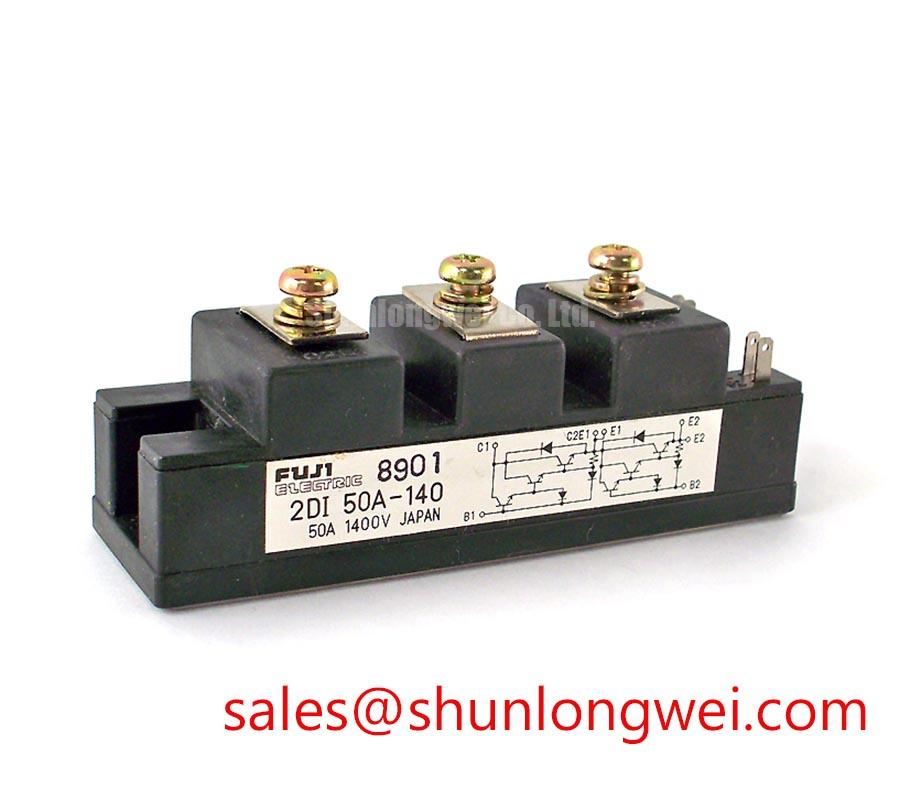
With the power stage isolated and its stored energy discharged, match the 2DI50A-140 terminal markings to the equipment schematic before applying a meter. Record diode-mode readings in both polarities with the module disconnected from parallel circuit paths, then compare them with an equivalent serviceable assembly under the same conditions. The specified collector, base and emitter characteristics identify this Fuji Electric device as a bipolar power transistor module; incoming inspection therefore needs to include its base circuit.
💡 Bench Tip: Record the meter polarity and base-terminal condition with every cold-test reading so that later comparisons remain meaningful. A diode-mode reading can help locate an abnormal conduction path, but it does not establish blocking capability, current gain or switching performance.
Trace the AC input protection through the rectifier and DC link before assessing the collector-emitter voltage exposure. IEC 61000-4-5 is the relevant surge immunity reference; it describes equipment testing rather than a standalone surge certification for this module. Design Consideration: evaluate MOV clamping, protective-device coordination and snubber placement against the actual equipment circuit and its required test conditions.
The official specifications establish VCEO at 1400 V, VCBO at 1400 V, continuous collector current IC at 50 A and collector power dissipation PC at 400 W, subject to the datasheet’s applicable rating conditions. Keep these ratings separate during assessment: collector power dissipation is a device thermal rating, while the permitted operating point depends on case temperature, cooling and the applicable safe operating area.
For incoming electrical checks at Tj of 25°C, the specified minimum DC current gain is hFE of 70 at IC of 50 A and VCE of 5 V. Maximum collector-emitter saturation voltage is 2.5 V at IC of 50 A and IB of 1 A; maximum base-emitter saturation voltage is 3.5 V. These are powered test characteristics, so a handheld meter cannot verify them directly.
Engineering Recommendation: assess fuse clearing behavior using the selected fuse’s time-current and I²t information alongside the semiconductor’s applicable withstand limits. Inspect terminal seating and heatsink contact, applying the mounting instructions for the exact assembly. For insulation assessment, distinguish collector blocking voltage from terminal-to-baseplate dielectric withstand. The Fuji Electric Power Semiconductors Portal provides the manufacturer’s power semiconductor documentation entry point.
Transient Dynamics & Electrical Design: Reverse Recovery Charge Temperature Coefficient on 2DI50A-140
Identify the commutation diode in the equipment schematic before attributing a reverse recovery waveform to the transistor module. Under the specified datasheet test conditions, the transistor switching specifications are maximum turn-on time of 3.0 μs, storage time of 15.0 μs and fall time of 3.0 μs. Storage time describes charge removal from the bipolar transistor; it is distinct from diode reverse recovery time.
Design Consideration: when investigating commutation current peaks, capture the diode current and switching-node voltage with suitable instrumentation, keeping load and temperature conditions comparable. Evaluate recovery behavior against the identified diode’s specifications. Neither recovery softness nor its temperature dependence follows from the transistor’s storage-time rating.
For replacement assessment, compare the 2DI300A-050-03 against the original device’s electrical and mechanical requirements. Its part number alone does not establish interchangeability.
| Assessment item | 2DI50A-140 | 2DI300A-050-03 |
|---|---|---|
| Collector-emitter voltage | 1400 V, official specification | Consult datasheet |
| Continuous collector current | 50 A under the specified rating conditions | Consult datasheet |
| Base-drive compatibility | Evaluate against specified gain and saturation conditions | Consult datasheet |
| Terminal arrangement and mounting | Match the original mechanical drawing | Compare drawings before substitution |
A medium-frequency induction melting or hardening furnace is a potential compatibility assessment context, subject to its converter topology, operating frequency and drive circuit. When mapping the surrounding power chain, evaluate the ETK85-060 separately against its intended circuit position and ratings; that association does not establish a matched module combination.
Preventing Spurious Faults: Turn-On Current Rise Limiting Guidelines for 2DI50A-140
Check the base-drive return path and turn-off waveform when unintended collector-current pulses appear. Design Consideration: reduce coupling between the power loop and control wiring, and assess base-drive impedance under switching conditions. Thyristor gate-trigger specifications and MOSFET gate-charge assumptions do not describe this transistor’s control interface.
Engineering Recommendation: evaluate an RC snubber against measured overshoot, ringing and resistor dissipation. Consider a series saturable reactor only where the converter topology supports it, with component selection determined by measured commutation behavior. Neither accessory has a universal value derived from the module’s voltage and current ratings.
Check driver timing against measured transistor charge removal across the intended operating conditions. The specified storage time warrants particular attention when assessing complementary switching and overlap current. Broader technology context is available in Future of Power Electronics; service acceptance should remain tied to device specifications and repeatable equipment measurements. Record the base waveform, collector-current transition and case temperature together when investigating a recurring switching fault.